Full exhaust Air_A1N_SOI MOSFETs part structure and its making method

A device structure and full depletion technology, applied in the field of microelectronics and solid-state electronics, can solve the problems of threshold voltage drift, device off-state current rise, etc., and achieve the effect of solving self-heating effect and suppressing short channel effect

Inactive Publication Date: 2009-05-20
XIAN UNIV OF TECH
View PDF3 Cites 0 Cited by
  • Summary
  • Abstract
  • Description
  • Claims
  • Application Information

AI Technical Summary

Problems solved by technology

[0003] The purpose of the present invention is to provide a fully depleted Air_AlN_SOI MOSFETs device structure, which not only solves the problem of self-heating effect of existing SOI devices, but also solves the device off-state current caused by the reduction of feature size and the introduction of high-K materials Problems with rising and threshold voltage drifting with drain voltage

Method used


Image

  • Full exhaust Air_A1N_SOI MOSFETs part structure and its making method
  • Full exhaust Air_A1N_SOI MOSFETs part structure and its making method
  • Full exhaust Air_A1N_SOI MOSFETs part structure and its making method

Examples


Embodiment Construction

[0020] The present invention will be described in detail below in conjunction with the accompanying drawings and specific embodiments.

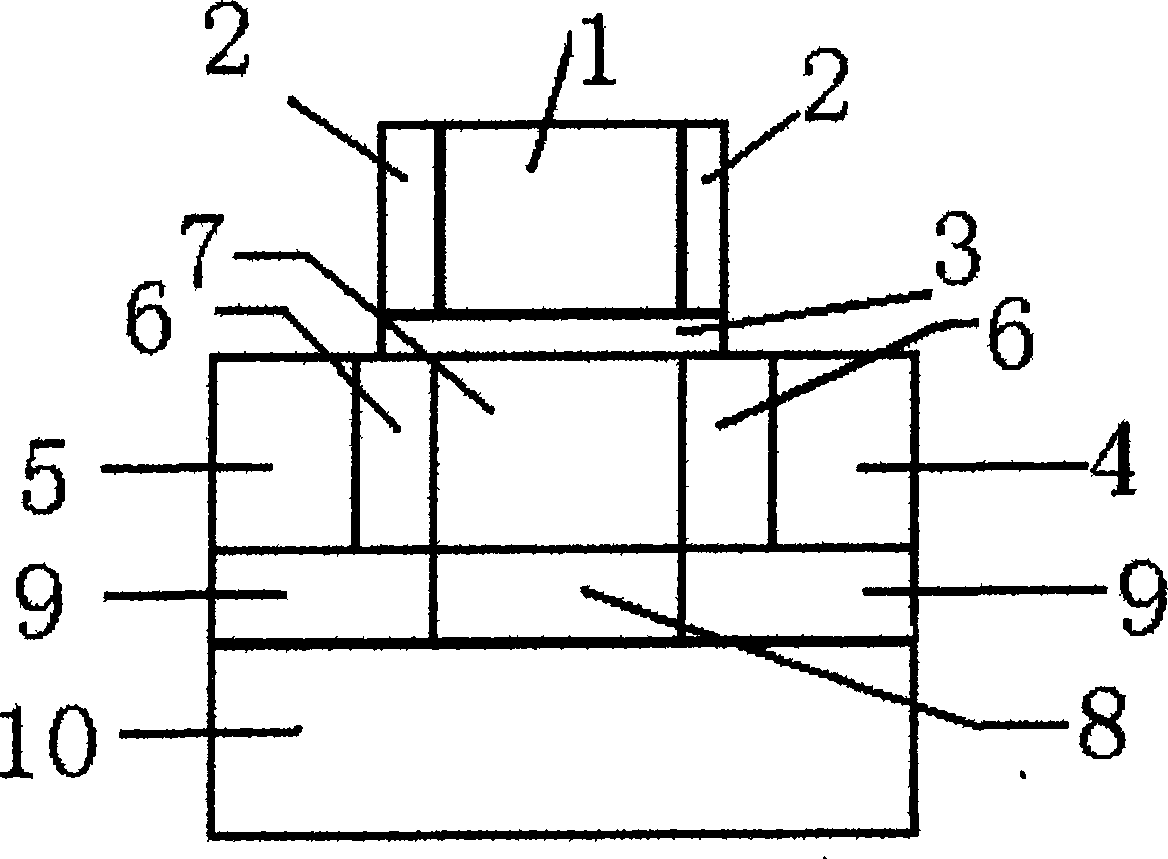
[0021] like figure 1 As shown, it is a schematic structural diagram of the present invention, and both sides of the gate 1 are provided with Si 3 N 4 Spacer 2, Gate 1 and Si 3 N 4 Below the side wall 2 is the gate oxide layer 3, one side of the lower layer of the gate oxide layer is the source region 4, and the other side of the lower layer of the gate oxide layer is the drain region 5, and the inner sides of the source and drain regions are provided with extended In region 6, the channel region 7 is directly under the gate oxide layer. Below the channel region is a cavity layer 8 , on both sides of the cavity layer 8 are insulating AlN materials 9 , and below the cavity layer 8 and the AlN insulating layer 9 is a layer of silicon substrate 10 .

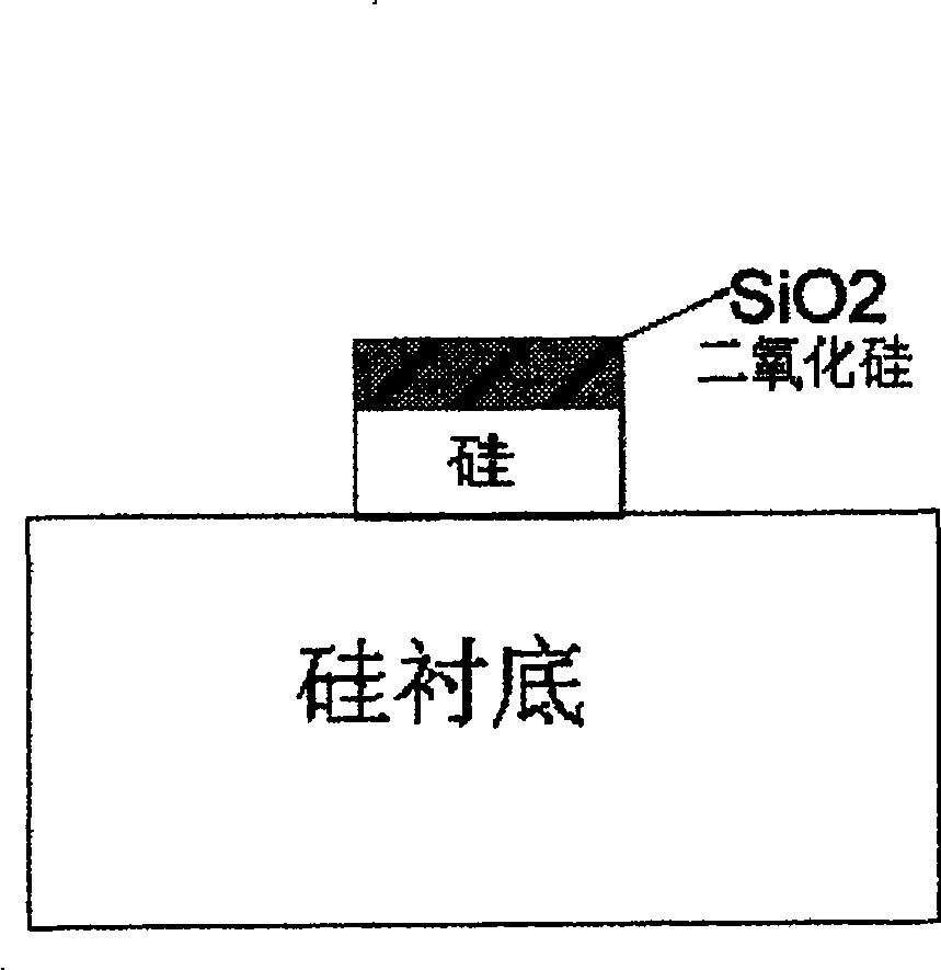
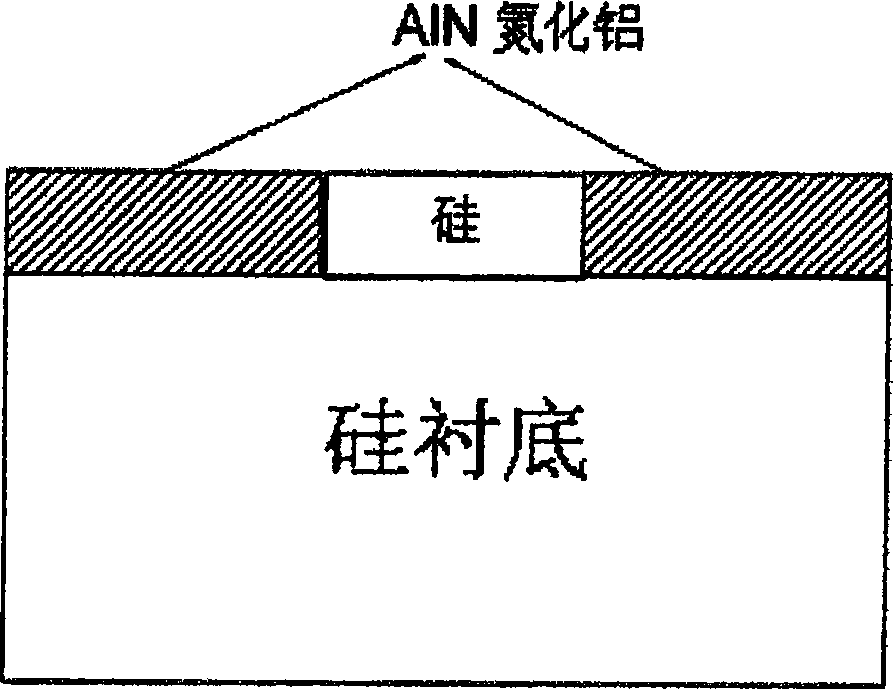
[0022] Air_AlN_SOI MOSFETs device structure of the present invention, its preparation can b...


PUM


Abstract

The invention discloses a total depletion Air A1N SPI MOSFETs device structure, which includes a grid and Si3N4 lateal walls. The grid and the Si3N4 lateral walls are arranged with a gate oxide on the lower part. A channel area is arranged below the gate oxide and is arranged with a source area and a drain area on both sides respectively. The inner sides of the source area and the drain area contacting with the channel area are arranged with an expansion area. An insulation layer and a silicon base are positioned below the channel area, the source area and the drain area in turn. The invention is characterized in that: the insulation layer consists of Air and A1N insulation layers arranged on both sides of Air, which is arranged below the channel area. By the silicon base prepared, perform isotropy on the silicon area on a silicon chip by a mask and form a hollow structure, and then use prior method to realize the upper part structure. The device structure can solve the problems of SOI device self-heating effect and increased leakage current and drifting threshold voltage in SOAN device at the same time.

Description

technical field [0001] The invention belongs to the technical field of microelectronics and solid electronics, and relates to a basic unit MOSFET of an integrated circuit, in particular to a fully depleted FD Air_AlN_SOI MOSFETs device structure, and also relates to a preparation method of the device structure. Background technique [0002] SOI devices have become a technology with great potential in deep submicron processes due to their advantages such as small parasitic capacitance, easy formation of shallow junctions, avoidance of latch-up effects, and good electrical characteristics. However, since the buried layer of the SOI device uses SiO with very low thermal conductivity 2 , so the heat generated in the channel region of the SOI device is difficult to dissipate smoothly when the circuit is working, causing heat to accumulate in the channel region, resulting in a decrease in drain current and a series of problems such as threshold voltage drift. The most effective w...

Claims


Application Information

Patent Timeline
Patent Type & Authority Patents(China)
IPC IPC(8): H01L29/786H01L21/336
Inventor 杨媛高勇巩鹏亮
Owner XIAN UNIV OF TECH
Why Eureka
Try Eureka