Preparation method of light emitting device

A technology for light-emitting devices and thin films, applied in semiconductor devices, electrical components, circuits, etc., can solve the problems of difficult epitaxial layers, high system costs, and poor yield of nano-structured devices

Inactive Publication Date: 2009-05-20
LG ELECTRONICS INC +1
View PDF4 Cites 2 Cited by
  • Summary
  • Abstract
  • Description
  • Claims
  • Application Information

AI Technical Summary

Problems solved by technology

However, there is a disadvantage in the growth process that it is very difficult to grow epitaxial layers of devices with nanostructures, and it is difficult to reproduce the shape of nanostructures with a predetermined length and thickness
[0019] Although fabrication of micro-LEDs and nanorod LEDs by photolithographically etching a patterned surface reduces stress, thereby improving light extraction efficiency, and enhancing internal efficiency, using semiconductor process technology (e.g., photolithography) Another disadvantage of the nanostructure fabrication method is poor yield and high system cost

Method used


Image

  • Preparation method of light emitting device
  • Preparation method of light emitting device
  • Preparation method of light emitting device

Examples


Embodiment Construction

[0038] The following will describe in detail in conjunction with the embodiments of the present invention with reference to the accompanying drawings.

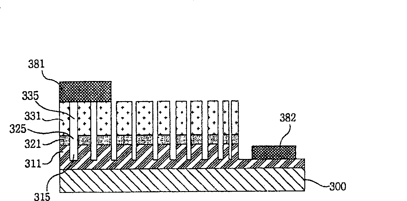
[0039] Figure 3a and 3b is a schematic sectional view of a light emitting device according to the present invention. refer to Figure 3a, the light emitting device comprises: a substrate (300); a first layer (311) having a first polarity formed on the substrate (300), a part of the first layer (311) is removed and a plurality of nanogrooves (315) are formed In the region where the first layer (311) is not removed; an active layer (321) formed on the unremoved first layer (311); formed on the active layer (321) and having a a second layer (331) of opposite polarity to the layer (311); a first electrode (381) formed on the second layer (331); and a second electrode formed on the removed first layer (311) (382).

[0040] The second layer (331) may further include a transparent electrode thereon, and the first electrode may ...


PUM


Abstract

A light emitting device and a method for fabricating the same are disclosed, whereby a thin mask film is changed to agglomerates by a simple thermal treatment process, and a plurality of nano openings, each opening spaced a distance apart, are formed in the agglomerates, a light emitting structure exposed to the nano openings is etched to form nano grooves and nano openings therein, enabling to enhance a light emitting area and to reduce the totally reflected light for an improvement of the light extraction efficiency.

Description

technical field [0001] The invention relates to a light emitting device and a manufacturing method thereof. Typically, a light emitting device is a light source having a certain wavelength, which is used for various purposes, for example, a light source and a display. Background technique [0002] Most light generated within a light emitting device is confined within the light emitting device by reflection above the critical angle at an interface between two materials, such as a semiconductor and air. That is, light incident on a surface at an angle greater than the critical angle will not pass through but be totally reflected (TIR). [0003] figure 1 is a conceptual illustration of an optical path formed between two materials due to different refractive indices according to the prior art. [0004] According to Snell's law of formula 1, when light is directed from a material with a refractive index n1 to another material with a refractive index n2, if the incident angle i...

Claims


Application Information

Patent Timeline
Patent Type & Authority Patents(China)
IPC IPC(8): H01L33/00H01L33/08
CPCH01L33/22H01L33/08H01L33/0095H01L2933/0083
Inventor 金钟旭曹贤敬
Owner LG ELECTRONICS INC
Why Eureka
Try Eureka