Chip electric connection structure and its manufacturing method

A technology of electrical connection and electrical connection pad, which is applied in the field of chip electrical connection structure and its manufacturing method, can solve the problems of poor electrical performance and reliability of the manufacturing process, simplify the manufacturing process and interface integration, and avoid electrical conduction and Molding, ensuring electrical performance and the effect of

Active Publication Date: 2009-06-24
PHOENIX PRECISION TECH CORP
View PDF10 Cites 0 Cited by
  • Summary
  • Abstract
  • Description
  • Claims
  • Application Information

AI Technical Summary

Problems solved by technology

[0013] Another object of the present invention is to provide a chip electrical connection structure and its manufacturing method, which avoids electrical defects and manufacturing processes caused by flip-chip and wire-bonding methods between existing semiconductor chips and circuit boards. reliability issues

Method used


Image

  • Chip electric connection structure and its manufacturing method
  • Chip electric connection structure and its manufacturing method
  • Chip electric connection structure and its manufacturing method

Examples


Embodiment

[0024] Figure 2A to Figure 2G It is a schematic cross-sectional view of the manufacturing method of the chip electrical connection structure of the present invention.

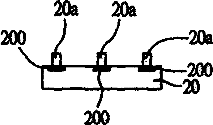
[0025] Such as Figure 2A As shown, at first, at least one semiconductor chip 20 is provided, and conductive bumps 20 a are formed on the electrode pads 200 of the semiconductor chip 20 . The conductive bump 20a may be formed by any one of the conductive metal group consisting of copper, gold, silver, tin, nickel and palladium or formed by laminating multiple layers of the above metals. According to practical experience, the metal bump is preferably made of copper, but not limited thereto. In addition, the conductive bump can be formed by means of electroplating, physical deposition or chemical deposition. Since the manufacturing method is not the main technical feature of the present invention, it will not be repeated here.

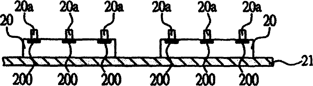
[0026] Such as Figure 2B As shown, at least one semiconductor chip 20 is mounte...


PUM


Abstract

This invention relates to chip electricity connection structure and its process method, which comprises the following steps: forming one semiconductor chip with conductive protruding block and connecting the semiconductor chip onto one load part; then forming one dielectric layer onto the semiconductor chip and its load parts and removing partly dielectric layer to expose conductive protruding block; forming electricity pad to get the conductive protruding block for circuit multiple layers process and connecting the chip onto outer electron parts.

Description

technical field [0001] The present invention relates to a chip electrical connection structure and a manufacturing method thereof, in particular to a conductive structure with electrical extension provided by electrode pads of a semiconductor chip and a manufacturing method thereof. Background technique [0002] With the evolution of semiconductor packaging technology, different packaging types have been developed for semiconductor devices, among which ball grid array (BGA) is an advanced semiconductor packaging technology, which uses a substrate to place semiconductor chips , and use Self-alignment technology to plant a plurality of solder balls arranged in a grid array on the back of the substrate, so that the same unit area of ​​the semiconductor chip carrier can accommodate more input / The output connection terminal (I / O connection) meets the needs of highly integrated semiconductor chips, and the entire packaging unit is soldered and electrically connected to the extern...

Claims


Application Information

Patent Timeline
Patent Type & Authority Patents(China)
IPC IPC(8): H01L21/60H01L23/488
CPCH01L24/19H01L2224/04105H01L2224/12105H01L2224/19H01L2224/32225H01L2224/32245H01L2224/73267H01L2224/92244H01L2924/14H01L2924/00H01L2924/00012
Inventor 许诗滨
Owner PHOENIX PRECISION TECH CORP
Why Eureka
Try Eureka