
Semiconductor device with tunable energy band gap

A technology of semiconductors and energy bands, applied in the direction of semiconductor devices, electrical solid devices, electrical components, etc.

Inactive Publication Date: 2009-07-08
KONINK PHILIPS ELECTRONICS NV
View PDF7 Cites 0 Cited by
  • Summary
  • Abstract
  • Description
  • Claims
  • Application Information

AI Technical Summary

Problems solved by technology

[0004] The remaining problem in U.S. Patent No. 4,935,935 is that the effect of changing the energy gap of the semiconductor is only maintained when a tuning voltage is applied to the piezoelectric film

Method used


Image

  • Semiconductor device with tunable energy band gap
  • Semiconductor device with tunable energy band gap
  • Semiconductor device with tunable energy band gap

Examples


Embodiment Construction

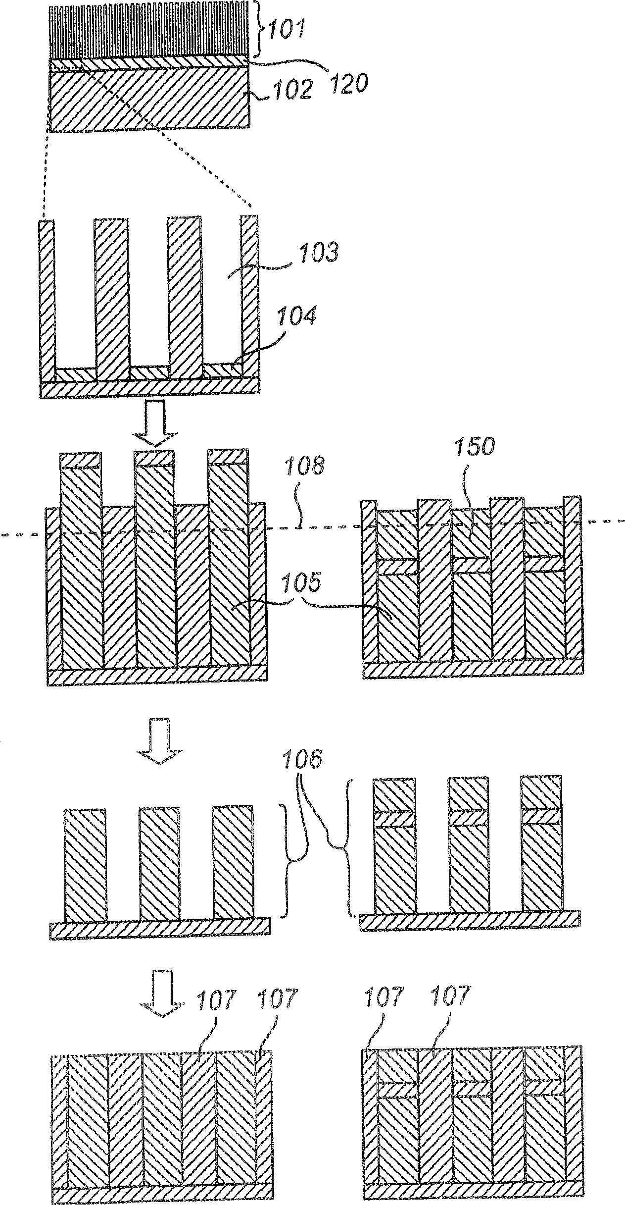
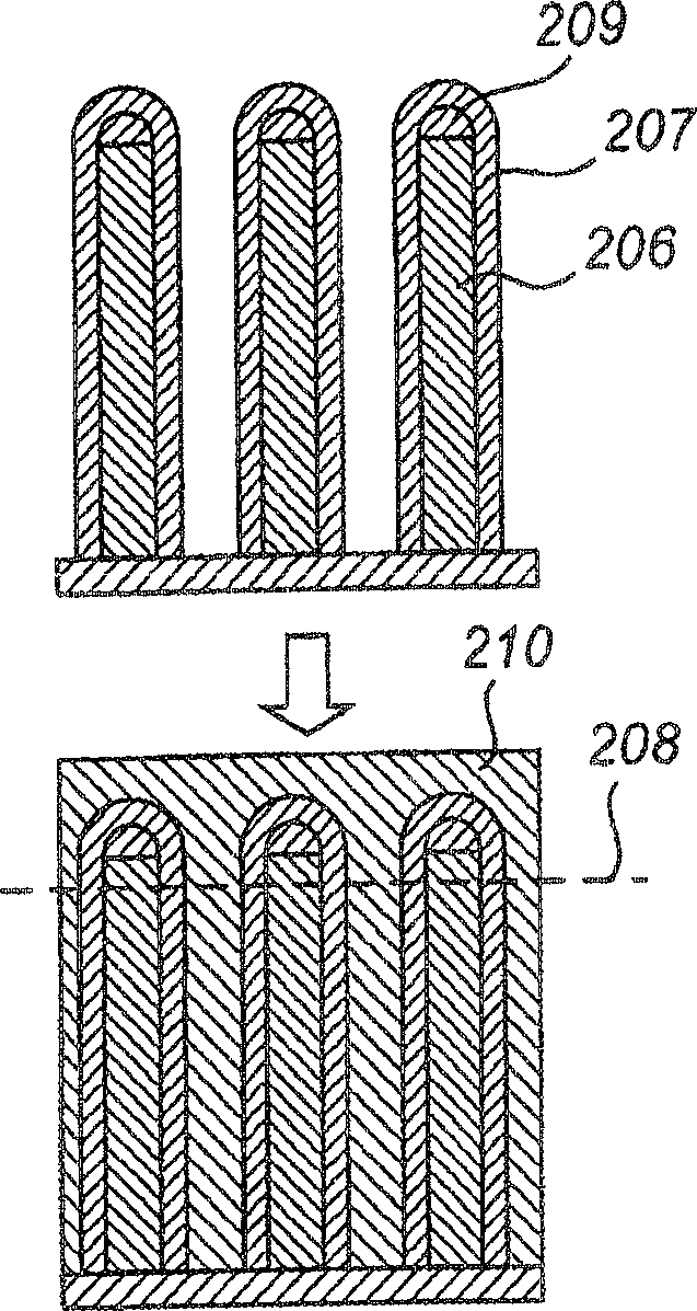
[0017] Semiconducting wires and carbon nanotubes can be grown by employing well-known vapor-liquid-solid (VLS) processes. This process is typically performed at a temperature in the range of 400 to 800°C. The VLS process uses small metal particles as nuclei for further growth. When using sufficiently small metal particles, the wire diameter can be made less than 10nm. As an alternative, semiconducting wires and metals can be deposited in suitable templates by electrochemical processes at room temperature. In either process, or a combination of both processes, segments of wires composed of, for example, n- and p-type semiconductor materials or exhibiting heterojunctions may be grown. Appropriate stencils can be used when high density semi-conductive lines are required. Electrochemical oxidation (ie, anodization) of aluminum is known to produce highly regular porous alumina when suitable conditions prevail. Typically, the holes are perpendicular to the surface of the substra...


PUM


Abstract

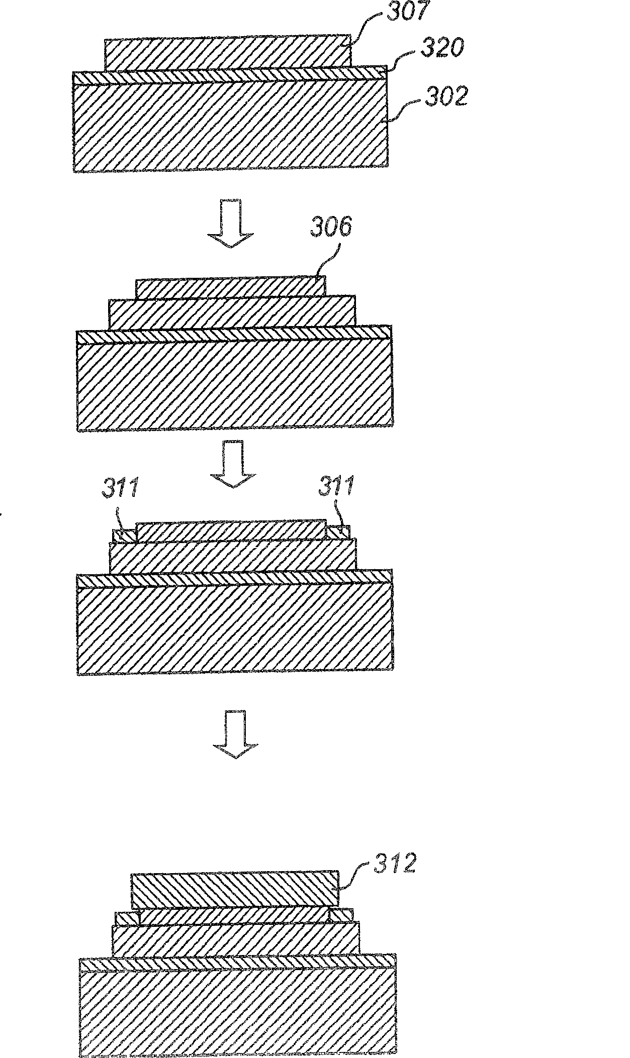
The present invention relates to a semiconductor device in which energy band gap can be reversibly varied. An idea of the present invention is to provide a device, which is based on a semiconducting material (306) in mechanical contact with a material that exhibits a reversible volume change when properly addressed, e.g. a phase change material (307). The device can, for example, be implemented in light emitting, switching and memory in applications. The semiconducting material can be reversibly strained by applying a local volume expansion to the phase change material. The resulting band gap variation of the semiconducting material can be utilized to tune the color of the light emitted from e.g. an LED or a laser. In other fields of application, contact resistance in semiconductor junctions can be controlled, and this feature is highly advantageous in memories and switches.

Description

technical field [0001] The present invention relates to semiconductor devices in which the energy bandgap can be reversibly changed. Background technique [0002] In semiconducting materials, the band gap is an important parameter, which largely determines the properties of semiconducting materials. The bandgap is defined as the energy difference between the top of the valence band and the bottom of the conduction band. This energy difference is the energy required to excite electrons from the valence band into the conduction band. Electrons in the conduction band are able to move through the material, thereby enabling electrical conductivity. Tuning of the bandgap of a light emitting diode (LED) results in a change in the color of the emitted light. When an electron in the conduction band falls back into the valence band, the electron releases energy in the form of a photon. The larger the band gap, the greater the energy of the photon. One way to reversibly tune the b...

Claims


Application Information

Patent Timeline
Patent Type & Authority Patents(China)
IPC IPC(8): H01S5/06H01L33/00
CPCH01L29/12B82Y10/00H01L27/15H01L29/0665H01L29/0676H01L29/0673
Inventor A·R·巴尔克南德E·P·A·M·巴克斯L·F·费纳
Owner KONINK PHILIPS ELECTRONICS NV
Learn More