Exposal machine carrying platform cleaning method and system

A technology for a film carrier and a film table is applied in the field of cleaning methods and systems for a film carrier of an exposure machine, which can solve the problems of wasting time and the like, and achieve the effects of high cleaning efficiency, time saving and utilization rate improvement.

Inactive Publication Date: 2009-07-22
SEMICON MFG INT (SHANGHAI) CORP +1
View PDF4 Cites 0 Cited by
  • Summary
  • Abstract
  • Description
  • Claims
  • Application Information

AI Technical Summary

Problems solved by technology

[0005] Therefore, the object of the present invention is to provide a cleaning method and system for the slide table of an exposure machine, to solve the time-wasting problem of the cleaning method for the slide table of an exposure machine

Method used


Image

  • Exposal machine carrying platform cleaning method and system
  • Exposal machine carrying platform cleaning method and system
  • Exposal machine carrying platform cleaning method and system

Examples


Embodiment Construction

[0034] In order to make the above objects, features and advantages of the present invention more comprehensible, specific implementations of the present invention will be described in detail below in conjunction with the accompanying drawings.

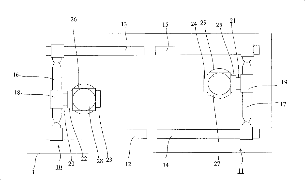
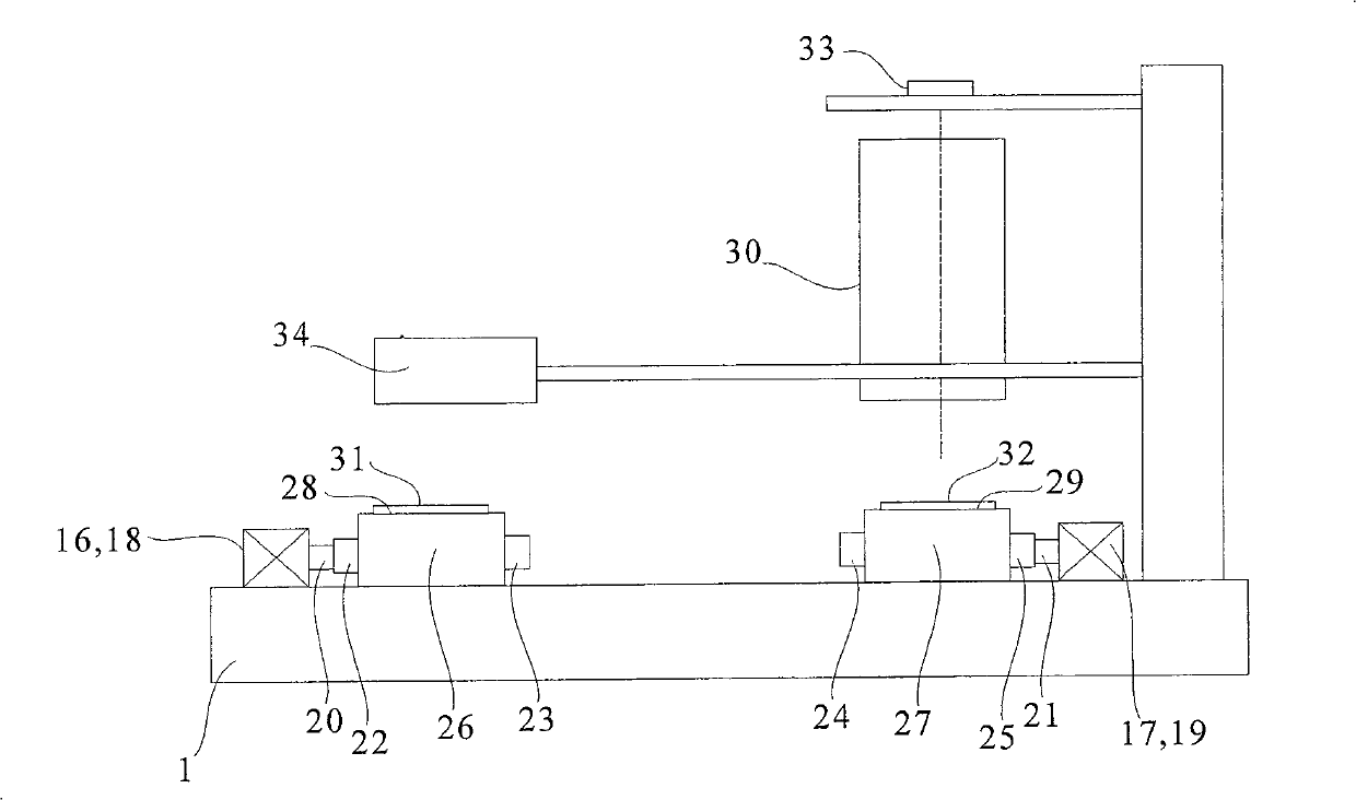
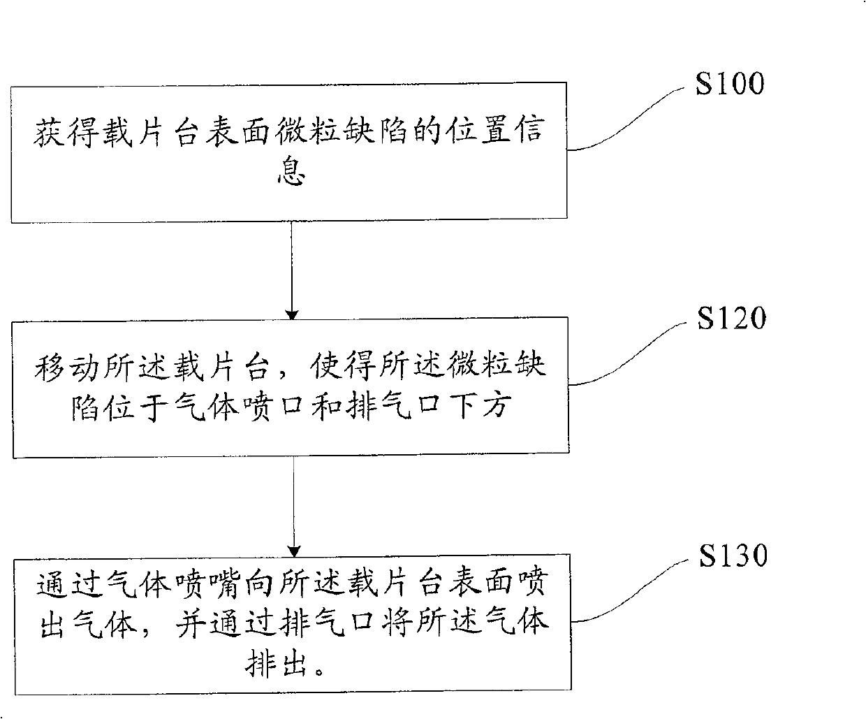
[0035] The invention discloses a method for cleaning the surface of the loading table of an exposure machine. The method judges the position information of particle defects on the surface of the loading table through the surface fluctuation information of the wafer on the loading table obtained during the exposure process, and according to the The position information moves the loading table so that the particle defects are located below the gas nozzle and the exhaust port, and the gas is ejected to the surface of the loading table through the gas nozzle, and the airflow of the ejected gas blows the The particle defects on the loading table are removed, and the gas with particle defects is discharged through the exhaust port. The metho...


PUM

PropertyMeasurementUnit
angleaaaaaaaaaa
diameteraaaaaaaaaa
diameteraaaaaaaaaa

Abstract

An exposure machine chip carrier surface cleaning method comprises the steps of obtaining particle defect position information of the surface of a chip carrier, moving the chip carrier according to the position information, positioning the particle defect below a gas nozzle and an exhaust port, spouting gas to the surface of the chip carrier through the gas nozzle and discharging the gas through the exhaust port. An exposure machine chip carrier surface cleaning system comprises a positioning device, a gas spouting pipe with the gas nozzle, an exhaust pipe with the exhaust port and a control device for controlling the gas spouting pipe to spout gas and controlling the exhaust pipe to discharge gas. The exposure machine chip carrier surface cleaning system and method of the present invention can save cleaning time, reduces the wear of a substrate under the exposure machine chip carrier, and improves the utilization ratio of exposure machines.

Description

technical field [0001] The invention relates to the technical field of semiconductor manufacturing, in particular to a method and system for cleaning a loading platform of an exposure machine in a photolithography process. Background technique [0002] The exposure equipment with twin stages has been successfully developed and applied to the production line of semiconductor manufacturing. The wafers are exposed and calibrated alternately through the two stages, which greatly improves the ability of the exposure machine to process wafers. US Patent No. US6262796B1 discloses a double-stage exposure machine and a double-stage structure applied to the exposure machine. figure 1 It is a schematic diagram of the structure of the double slide stage disclosed in the US patent. Such as figure 1 As shown, the double slide stage structure has two oppositely placed "H" shaped guide rails 10, 11 on the base 1, and the guide rail 10 has two guide bars 12, 13 placed in parallel and one w...

Claims


Application Information

Patent Timeline
Patent Type & Authority Patents(China)
IPC IPC(8): G03F7/20H01L21/00B23Q1/00B08B5/00
Inventor 黄良志
Owner SEMICON MFG INT (SHANGHAI) CORP
Why Eureka
Try Eureka