Method for producing a multilayer printed wiring board
A technology of printed circuit and manufacturing method, which is applied in multilayer circuit manufacturing, printed circuit manufacturing, printed circuit, etc., and can solve problems such as damage to flexible parts, time-consuming operation, and undulation of flexible parts
- Summary
- Abstract
- Description
- Claims
- Application Information
AI Technical Summary
Problems solved by technology
Method used
Image

Examples
Embodiment Construction
[0056] Hereinafter, a method of manufacturing a multilayer printed wiring board according to an embodiment of the present invention will be described with reference to the drawings.
[0057] Implementation form 1
[0058] In this implementation form according to Figure 1 to Figure 9 A manufacturing method for manufacturing a multilayer printed circuit wiring board will be described.
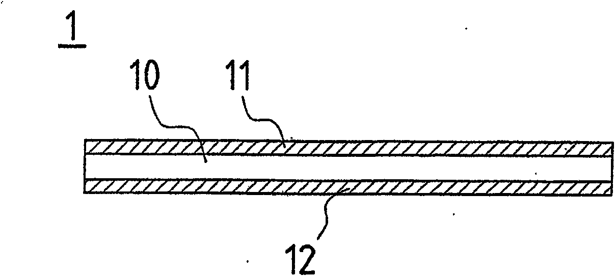
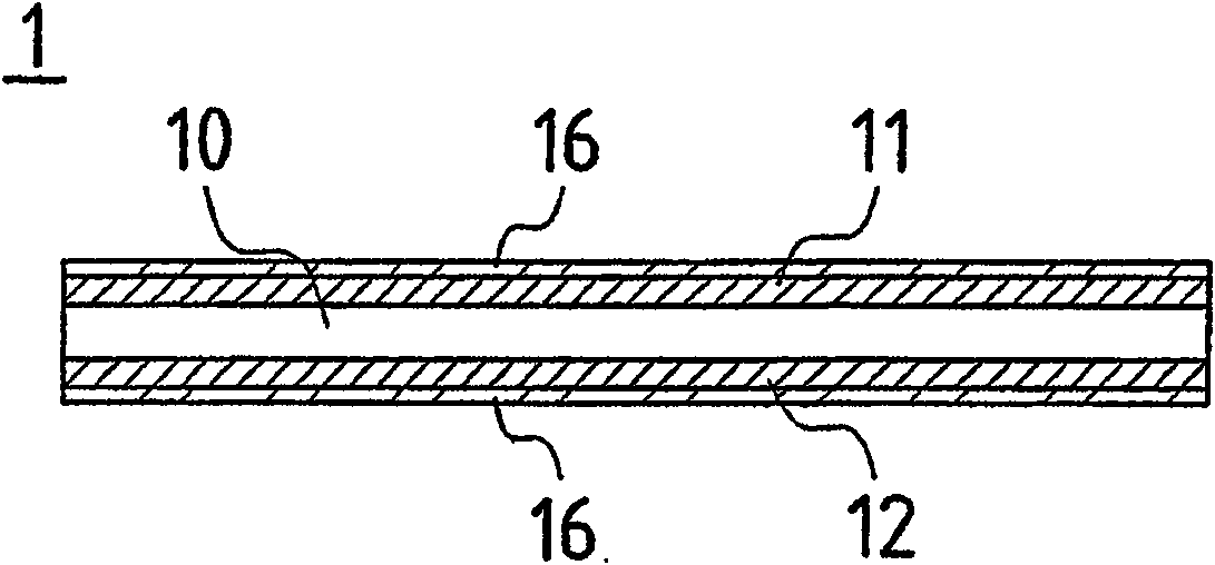
[0059] figure 1 It is a cross-sectional view of a core board in the method of manufacturing a multilayer printed wiring board according to Embodiment 1 of the present invention. The core board 1 is formed by laminating conductor layers 11 and 12 on both sides of a flexible insulating resin film 10 with an adhesive. The insulating resin film 10 is formed of flexible polyimide resin, polyether ketone, liquid crystal polymer resin, or the like. For the conductor layers 11, 12, copper foil is used. In addition, the conductor layers 11 and 12 may be formed using metal foil other than copper foi...
PUM
 Abstract
Description
Claims
Application Information
 - R&D
- Intellectual Property
- Life Sciences
- Materials
- Tech Scout
- Unparalleled Data Quality
- Higher Quality Content
- 60% Fewer Hallucinations
Browse by: Latest US Patents, China's latest patents, Technical Efficacy Thesaurus, Application Domain, Technology Topic, Popular Technical Reports.
© 2025 PatSnap. All rights reserved.Legal|Privacy policy|Modern Slavery Act Transparency Statement|Sitemap|About US| Contact US: help@patsnap.com