Dielectric substrate integrated waveguide slot array antenna

A slot array antenna, dielectric substrate technology, applied in slot antennas, antennas, antenna arrays and other directions, can solve the problems of high processing cost, high antenna cost, increased mechanical cost, etc., to improve directional radiation capability, cross-polarized electrical The effect of low level and high manufacturing precision

Inactive Publication Date: 2009-08-19
SOUTHEAST UNIV
View PDF3 Cites 0 Cited by
  • Summary
  • Abstract
  • Description
  • Claims
  • Application Information

AI Technical Summary

Problems solved by technology

[0003] 1) Large size, heavy weight, difficult to move
[0004] 2) The material cost is high, the processing cost is expensive, and the related mechanical cost increases due to its difficulty in moving
[0005] 3) The manufacturing accuracy cannot guarantee the normal operation of the antenna, so after the processing is completed, an adjustment process is required to correct the error
These defects make this type of antenna very expensive

Method used


Image

  • Dielectric substrate integrated waveguide slot array antenna
  • Dielectric substrate integrated waveguide slot array antenna
  • Dielectric substrate integrated waveguide slot array antenna

Examples


Embodiment 1

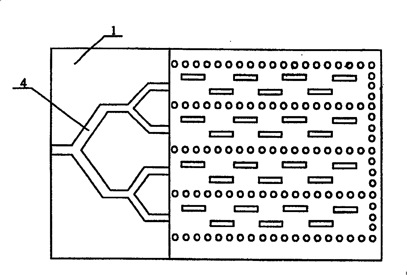
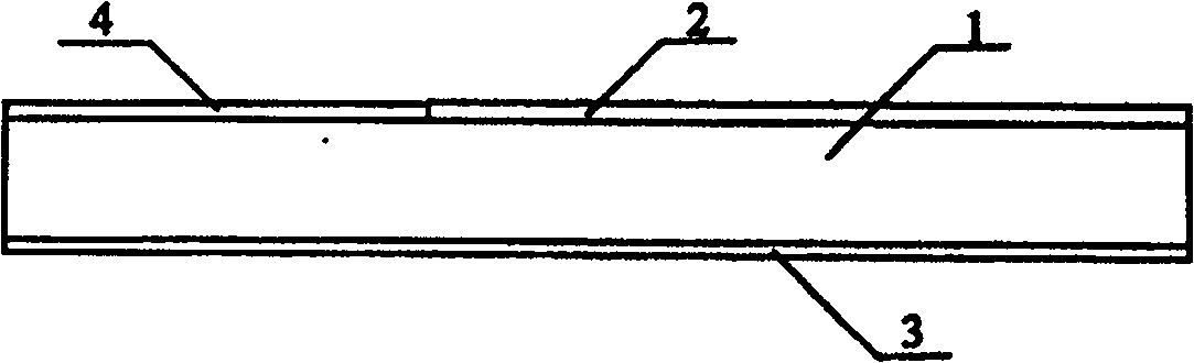
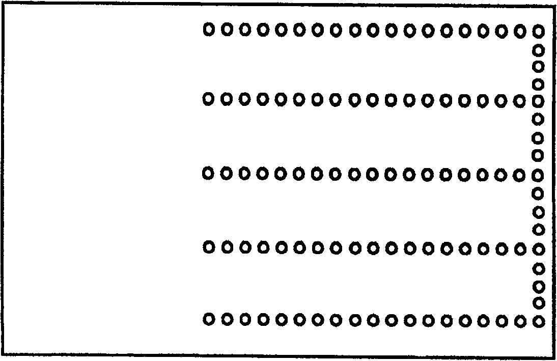
[0023] A dielectric substrate integrated waveguide slot array antenna for electronic equipment such as wireless communication, radar, electronic navigation and electronic countermeasures, including a dielectric substrate plate 1, wherein a complete metal foil 3 is provided on the back of the dielectric substrate plate 1, A slot array 2 and a microstrip power divider 4 are etched on the front metal foil, the slot array array 2 is connected to the microstrip power divider 4, and an intercommunication through hole 5 is provided in the dielectric substrate plate 1, and the through hole 5 The metallized through holes are arranged in a "U" shape, and the metallized through holes arranged in a "U" shape surround the slot array unit.

Embodiment 2

[0025] This embodiment implements the dielectric substrate integrated waveguide slot array antenna described above at 10 GHz. The dielectric length of the dielectric substrate is equal to 2.4, the thickness is 1.5 mm, and the loss tangent is less than one thousandth. The diameter of the metal through hole used to form the dielectric integrated waveguide is 1 mm, the distance between the through holes is 2 mm, the width of the dielectric substrate integrated waveguide is 12.46 mm, and the distance between adjacent dielectric substrate integrated waveguides is 2.54 mm. The width of the microstrip line is 2.4mm, and the power divider is divided into two stages, one divided into two, and two divided into four. The length of the branch line is 5.40mm, and the width is equal to 1.19mm.

[0026] A total of 16 slits of 4X4 ​​are etched on the metal surface of the dielectric substrate. The length of each slot and the displacement relative to the centerline of the waveguide can be seen...


PUM


Abstract

The invention discloses a dielectric substrate integrated waveguide slot array antenna used for electronic equipment such as wireless communication, radar, electronic navigation and electronic countermeasures. The metal foil on one side is etched with a slot array and a microstrip power divider, the slot array unit is connected to the microstrip power divider, and a through hole is provided on the dielectric substrate board and the metal foil, and the through hole is Metallized through holes, the metallized through holes are arranged in a "U" shape, and the metallized through holes arranged in a "U" shape surround the slot array unit; the present invention has the following advantages: easy to produce, especially easy to mass produce and The manufacturing precision is high and the performance of the antenna can be improved.

Description

technical field [0001] The invention relates to an antenna that can be used in antennas and feed modules of communication systems, in particular to a dielectric substrate integrated waveguide slot array antenna. Background technique [0002] The traditional metal waveguide slot array antenna has excellent characteristics such as narrow main lobe width, shapeable pattern, and low cross-polarization level, and is widely used in microwave and millimeter wave radar and communication systems. A complete metal waveguide slot array antenna system is composed of multiple metal waveguides, some of which are slotted on the wall to form a slot array, and the other part of the waveguide is used as a feed network. This inevitably has some drawbacks: [0003] 1) It is bulky, heavy and difficult to move. [0004] 2) The material cost is high, the processing cost is expensive, and the related mechanical cost increases due to the difficulty in moving it. [0005] 3) The manufacturing accu...

Claims


Application Information

Patent Timeline
Patent Type & Authority Patents(China)
IPC IPC(8): H01Q1/38H01Q13/08H01Q13/10H01Q21/00
Inventor 洪伟颜力吴柯陈继新华光
Owner SOUTHEAST UNIV
Why Eureka
Try Eureka