Edge electrical field switching type liquid crystal display and manufacture method thereof
A technology of fringe electric field switching and liquid crystal display, applied in instruments, nonlinear optics, optics, etc., can solve problems such as image retention and imbalance, and achieve the effect of reducing the number and improving image retention
- Summary
- Abstract
- Description
- Claims
- Application Information
AI Technical Summary
Problems solved by technology
Method used
Image

Examples
no. 1 example
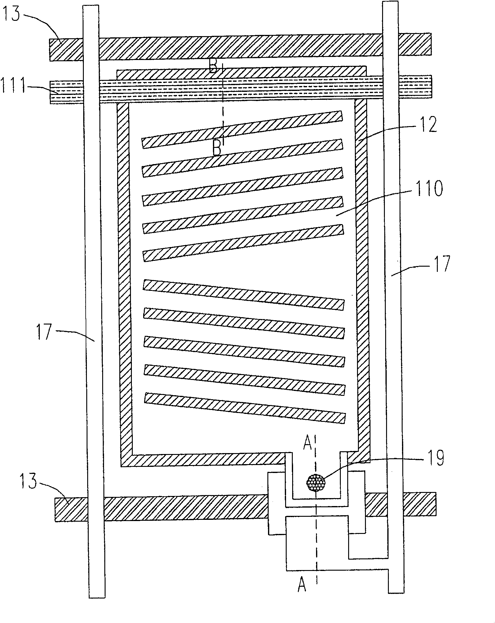
[0049] see Figure 2A , which is a schematic plan view of a certain pixel area in the first embodiment provided by the present invention. Each pixel area is formed by interlacing several gate lines 22 and several data lines 272 to surround each other, and includes: a common electrode 26, a pixel electrode 210 with several openings, a common line 271 parallel to the data line 272 and a contact hole 29 .
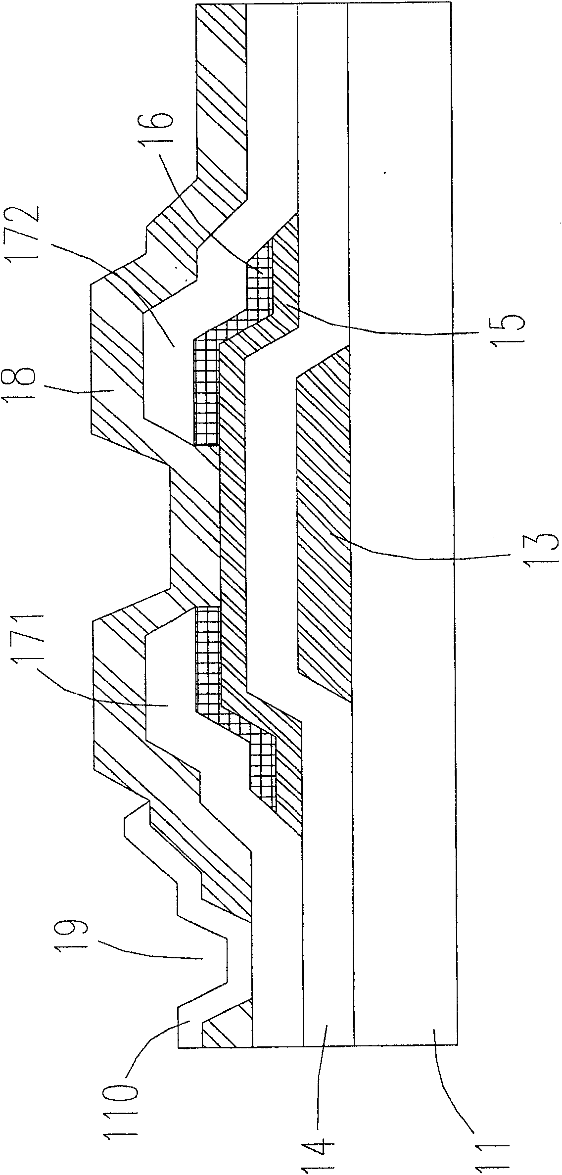
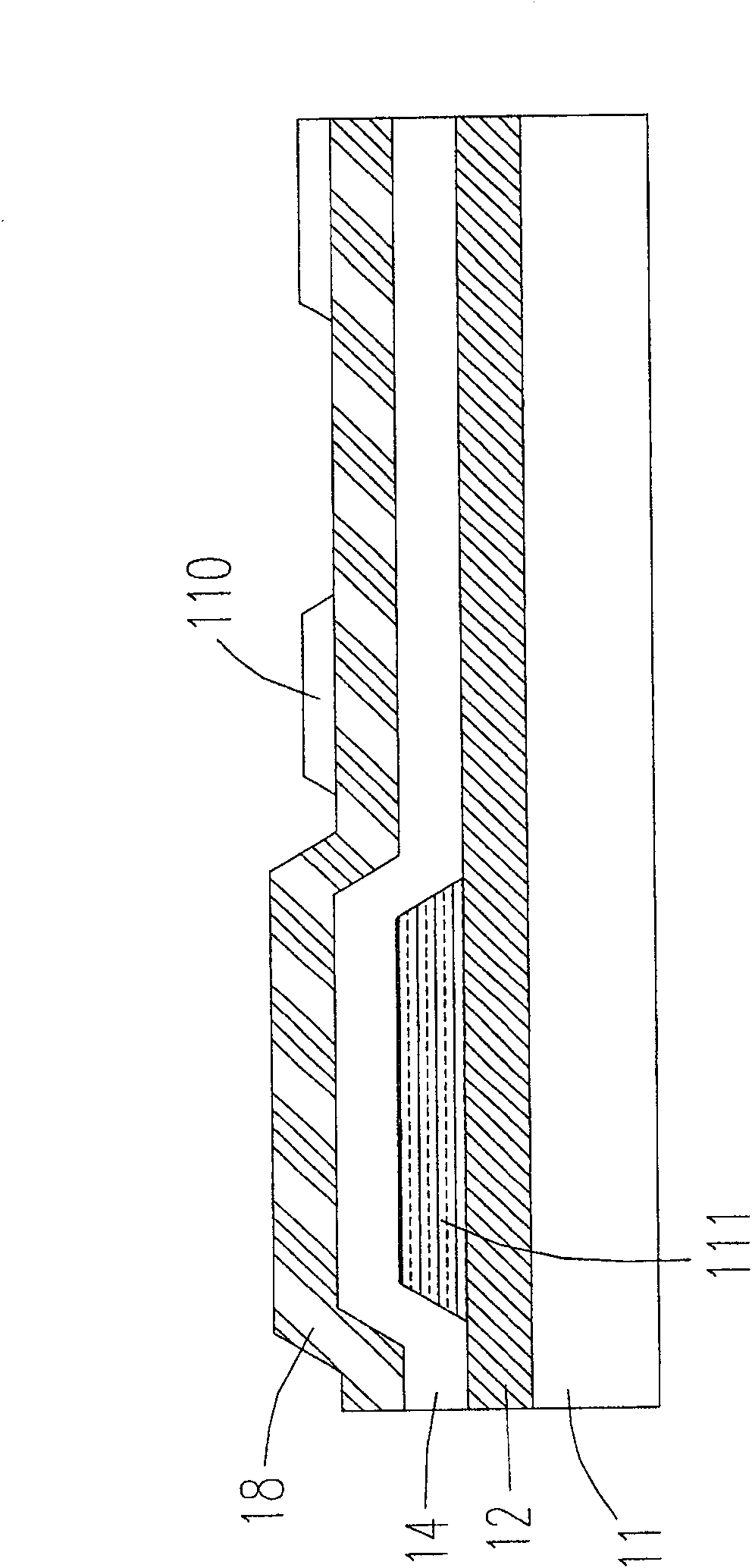
[0050] see Figure 2B ,for Figure 2A A schematic cross-sectional view along line A-A. The first embodiment provided by the present invention and its manufacturing method are described as follows. Firstly, a substrate 21 is provided, and a first metal layer is formed thereon. Next, the first metal layer is etched to form several gate lines 22 , and then a gate insulating layer 23 is coated to cover the gate lines 22 and part of the substrate 21 . Then, the channel portion 24 , the doped portion 25 and the common electrode 26 are sequentially formed on the gate insulating...
no. 2 example
[0053] Figure 3A to Figure 3E It is a fringe field switching liquid crystal display according to the second embodiment of the present invention, which utilizes the half-tone technology process (Half-Tone Technology Process) to simultaneously define the process schematic diagram of the common electrode and the data line. in, Figure 3A to Figure 3E The right half of Figure 2A A schematic sectional view along line A-A, and its left half is Figure 2A A schematic sectional view along line B-B.
[0054] first as Figure 3A As shown, a semiconductor layer and a doped layer are formed on the gate insulating layer 23 and the substrate 21 in sequence. Next, the semiconductor layer and the doped layer are etched to form the channel portion 24 and the doped portion 253 above a gate line 22 . Furthermore, a first transparent conductive layer 261 is formed on the doped portion 253 and the gate insulating layer 23 , and a second metal layer 2711 is formed thereon. Wherein, the firs...
no. 3 example
[0060] see Figure 4A , which is a schematic plan view of a certain pixel area in the third embodiment provided by the present invention. Each pixel area is formed by interlacing several gate lines 42 and several data lines 462 to surround each other, and includes: a common electrode 47, a pixel electrode 410 with several openings, a gate parallel to the data lines 462 The common line 461 and a contact hole 49 .
[0061] see Figure 4B ,for Figure 4A A schematic cross-sectional view along line A-A. Now the third embodiment provided by the present invention and its manufacturing method are described as follows. Firstly, a substrate 41 is provided, and a first metal layer is formed thereon. Secondly, the first metal layer is etched to form several gate lines 42 , and then a gate insulating layer 43 is coated to cover the gate lines 42 and part of the substrate 41 . Then, the channel portion 44 and the doped portion 45 are sequentially formed on the gate insulating layer 4...
PUM
 Abstract
Description
Claims
Application Information
PatSnap Eureka turns technology decisions into work you can execute. Powered by our Innovation Knowledge Graph, it runs expert workflows across engineering, life sciences, materials and intellectual property. Get your review-ready output in minutes.


