Light-emitting device with increased quantum efficiency

A technology of light-emitting devices and light-emitting layers, which is applied in the fields of electric solid-state devices, semiconductor devices, semiconductor/solid-state device manufacturing, etc., can solve problems such as loss and quantum efficiency decline, and achieve the effect of precise adjustment

Active Publication Date: 2009-10-28
KONINKLIJKE PHILIPS ELECTRONICS NV
View PDF5 Cites 0 Cited by
  • Summary
  • Abstract
  • Description
  • Claims
  • Application Information

AI Technical Summary

Problems solved by technology

The excited molecules are thus quenched and the quantum efficiency of the OLED drops
These reactions are a large source of loss in O

Method used


Image

  • Light-emitting device with increased quantum efficiency
  • Light-emitting device with increased quantum efficiency
  • Light-emitting device with increased quantum efficiency

Examples


Embodiment

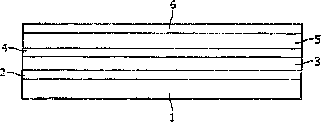
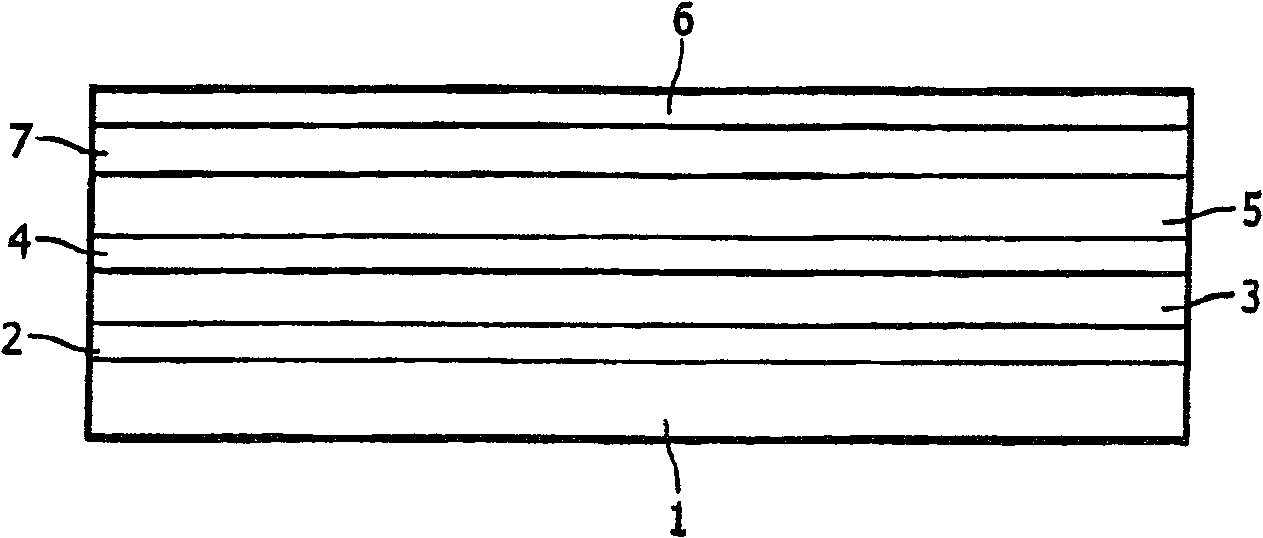
[0040] On a transparent substrate 1 made of glass, ITO with a layer thickness of 150 nm was applied as anode 2 . α-NPD with a layer thickness of 30 nm was applied as first hole-transport layer 3 on the anode 2 by spin coating. A BCP first hole-blocking layer 4 with a layer thickness of 1 nm is applied on the hole-transport layer 3 . On the first hole blocking layer 4 is applied an emitting layer 5, i.e. Ir(ppy) embedded in TCTA 3 . The layer thickness of the light emitting layer 5 was 30 nm. A 10 nm-thick second hole-blocking layer 7 of BCP is applied on the emitting layer 5 . Alq was applied with a layer thickness of 40 nm on the second hole blocking layer 7 3 as the electron transport layer 12. A 151.5-nm-thick cathode 6 consisting of a 1.5-nm-thick lithium benzoate first layer and a 150-nm-thick aluminum second layer is applied to the electron-transport layer 12 .

[0041] Compared with the light emitting device without the first hole blocking layer 4, the quantum eff...


PUM


Abstract

The invention describes a light-emitting device comprising at least a substrate (1), an anode (2), a first hole-transport layer (3), a light-emitting layer (5) and a cathode (6), wherein the first hole-blocking layer (4 ) is disposed between the first hole transport layer (3) and the light emitting layer (5). The hole blocking layer (4) reduces the concentration of holes reaching the emissive layer (5), so that the concentration of holes, which are usually the main charge carriers, can be matched to the electron current.

Description

technical field [0001] The present invention relates to a light emitting device comprising at least a substrate, an anode, a hole transport layer, a light emitting layer and a cathode. Background technique [0002] Electronically controlled display systems are widely known and used in various embodiments based on various principles. [0003] One principle uses organic light-emitting diodes, so-called OLEDs, as light sources. Organic light emitting diodes include multiple functional layers. Typical structures of OLEDs are described in "Philips Journal of Research, 1998, 51, 467". A typical structure includes an ITO (Indium Tin Oxide) layer as transparent electrode (anode), a conductive polymer layer, an electroluminescent layer containing luminescent material and an electrode (cathode) consisting of a metal, preferably a metal with a low work function. Such structures are usually applied on a substrate, usually glass. The generated light passes through the substrate to th...

Claims


Application Information

Patent Timeline
IPC IPC(8): H01L51/50H01L51/00H01L51/30H01L51/40H01L51/52
CPCH01L51/5096H01L51/002H01L51/005H01L51/0059H01L51/5092H01L51/5088H01L51/0051H10K71/30H10K85/611H10K85/60H10K85/631H10K50/171H10K50/18H10K50/17
Inventor H·F·贝尔纳W·布泽尔特D·贝特拉姆
Owner KONINKLIJKE PHILIPS ELECTRONICS NV
Why Eureka
Try Eureka