Semiconductor element and its producing method

A manufacturing method and semiconductor technology, applied in semiconductor/solid-state device manufacturing, semiconductor devices, electrical components, etc., can solve the problems of embedded MIM capacitor limitation, chip area reduction, and inability to provide capacitance value, etc.

Active Publication Date: 2007-07-25
NEXCHIP SEMICON CO LTD
View PDF0 Cites 6 Cited by
  • Summary
  • Abstract
  • Description
  • Claims
  • Application Information

AI Technical Summary

Problems solved by technology

However, under the trend of increasing integration, the available chip area of ​​the capacitor plate (Plate) is forced to reduce, and the increasing function of active components makes the number of capacitors continue to increase. These problems are the application of MIM capacitors. bottleneck
Due to the current dielectric material and plate area available for MIM capacitors cannot provide sufficient capacitance (for example, 0.75fF / um is required for an input voltage of 18V 2 ) to deal with voltage regulation problems at higher input voltages
Therefore, there are obvious limitations in the way in which embedded MIM capacitors can be placed in order to stabilize the input voltage

Method used


Image

  • Semiconductor element and its producing method
  • Semiconductor element and its producing method
  • Semiconductor element and its producing method

Examples


Embodiment Construction

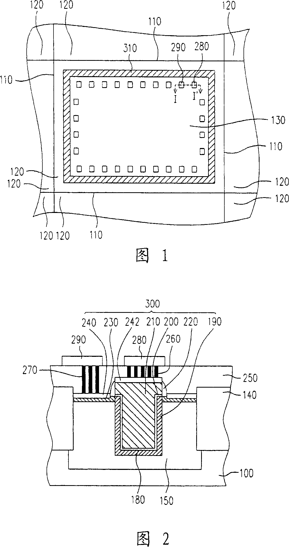
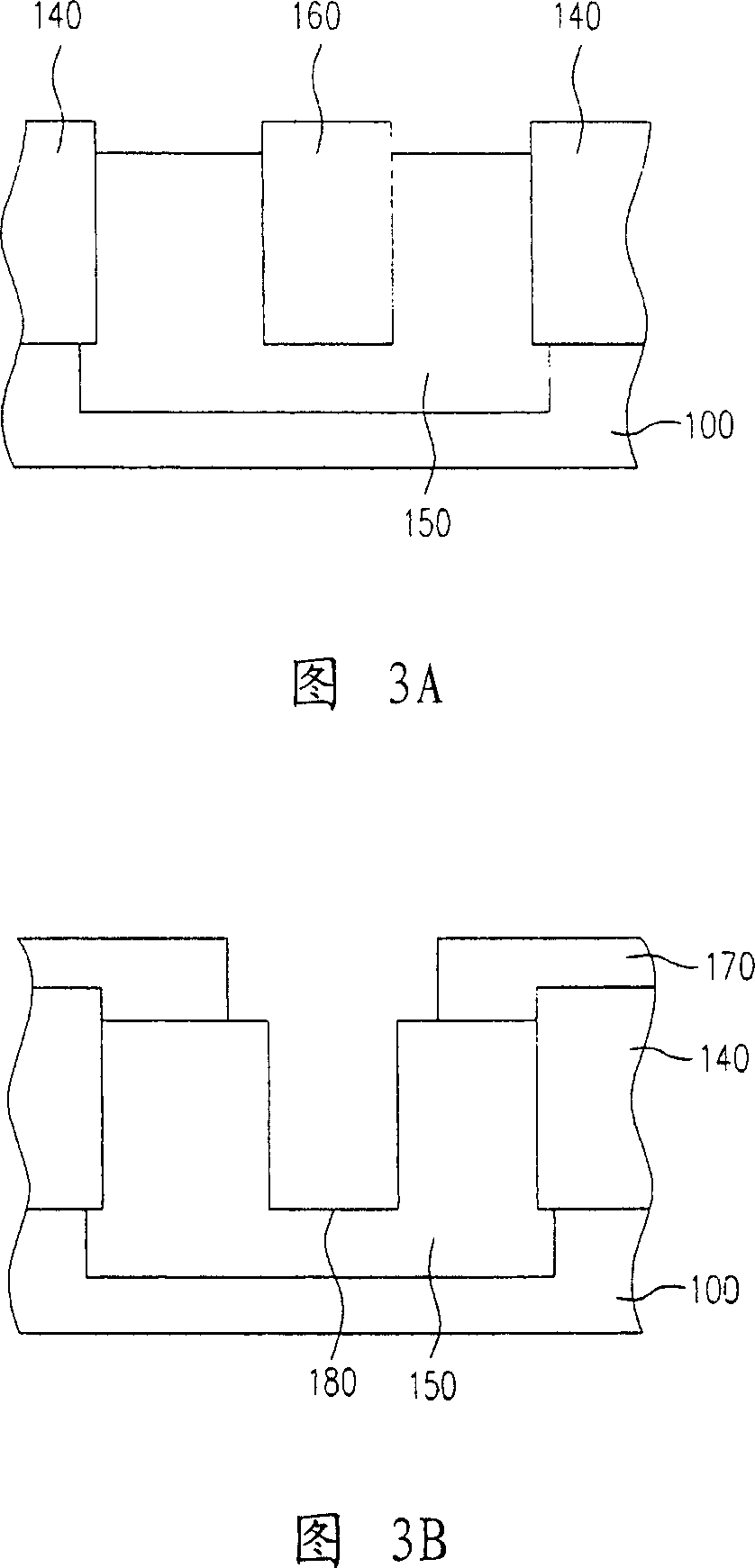
[0048] Fig. 1 is a top view of a semiconductor element of a preferred embodiment of the present invention. Referring to FIG. 1 , the semiconductor device of the present invention is composed of a substrate 100 , a plurality of pads and a trench capacitor 300 . There are a plurality of dicing lines 110 on the substrate 100 , and the dicing lines 110 divide the substrate 100 into a plurality of chips 120 . That is, the area divided by the dicing line 110 is the chip area to be diced in the future. A peripheral area of ​​the chip 120 has a plurality of bonding pads, including a bonding pad 280 and a bonding pad 290 . The trench capacitor 300 shown in FIG. 2 is disposed under the pad, or in the area 310 between the pad and the cutting line 110 . In this embodiment, the trench capacitor 300 located under the pads 280 and 290 is taken as an example for illustration.

[0049]Please continue to refer to Fig. 2, which is a cross-sectional view along the section line I-I' in Fig. 1 ....


PUM


Abstract

First, the method provides substrate. Cut line on the substrate divides the substrate into at least one chip. Being formed on the substrate, grooves are positioned on prearranged area, where weld pads are to be formed, or on the area between pads and the cut line. Low electrode is formed on sidewall of substrate, and in substrate of base. Dielectric layer of capacitance and up electrode are formed on the substrate. The up electrode is filled in the grooves. Then, being formed on the substrate, the doping area is connected to the low electrode electrically. Afterwards, first weld pad and second weld pad are formed on the substrate. Through the doping area, the low electrode is connected to the first weld pad electrically, and the up electrode is connected to the second weld pad electrically. Since capacitor is formed under pads, or on the substrate between pads and the cut line, the invention reduces area engaged by chip.

Description

technical field [0001] The invention relates to a semiconductor element and a manufacturing method thereof, in particular to a high-voltage semiconductor capacitor and a manufacturing method thereof. Background technique [0002] With the advancement of integrated circuit manufacturing, the size of components has been continuously reduced, and metal oxide semiconductor (MOS) has become the main component of circuit design. However, since the operating voltage of the MOS transistor is getting smaller and smaller, it is easy to be damaged due to the intrusion of external noise. Industry and academia have devoted a lot of effort to the prevention of noise, and many solutions have been obtained. [0003] When the input voltage is applied to the high-voltage components through the input pad (Input Pad), there will be similar noise problems. In order to stabilize the input voltage of the high-voltage component, a capacitor with a large capacitance (Capacitance) is arranged on th...

Claims


Application Information

Patent Timeline
Patent Type & Authority Applications(China)
IPC IPC(8): H01L27/02H01L21/82
Inventor 陈文吉陈东波艾世强
Owner NEXCHIP SEMICON CO LTD
Why Eureka
Try Eureka