Eureka AIR delivers breakthrough ideas for toughest innovation challenges, trusted by R&D personnel around the world.

Solid-state imaging apparatus and method for driving the same

A solid-state imaging device and solid-state imaging element technology, which is applied to the field of white spots during long-second accumulation, can solve problems such as white spot generation, hindering charge readout, and reverse injection, and achieves the effect of preventing white spot and high practical value

Inactive Publication Date: 2007-07-25
PANASONIC CORP
View PDF0 Cites 0 Cited by
  • Summary
  • Abstract
  • Description
  • Claims
  • Application Information

AI Technical Summary

Problems solved by technology

[0013] However, in the conventional driving method, when holes are accumulated directly under the readout gate to prevent the increase of dark current, if the holes are excessively accumulated, the potential of the semiconductor substrate will be unstable, and it is easy to occur from the semiconductor substrate to the The case of photodiode reverse injection of unwanted charges
[0014] That is, in the long-second accumulation mode (hereinafter also referred to as the long-term accumulation mode) in which the photodiode accumulates charges for more than two vertical periods, not only the potential of the semiconductor substrate is shifted due to the accumulated holes, and white spots are generated, but also It also hinders the readout of the charge accumulated in the photodiode, injects unnecessary charges into the channel of the vertical CCD, and hinders the transfer of the readout charge

Method used


Image

  • Solid-state imaging apparatus and method for driving the same
  • Solid-state imaging apparatus and method for driving the same
  • Solid-state imaging apparatus and method for driving the same

Examples


Embodiment approach 1

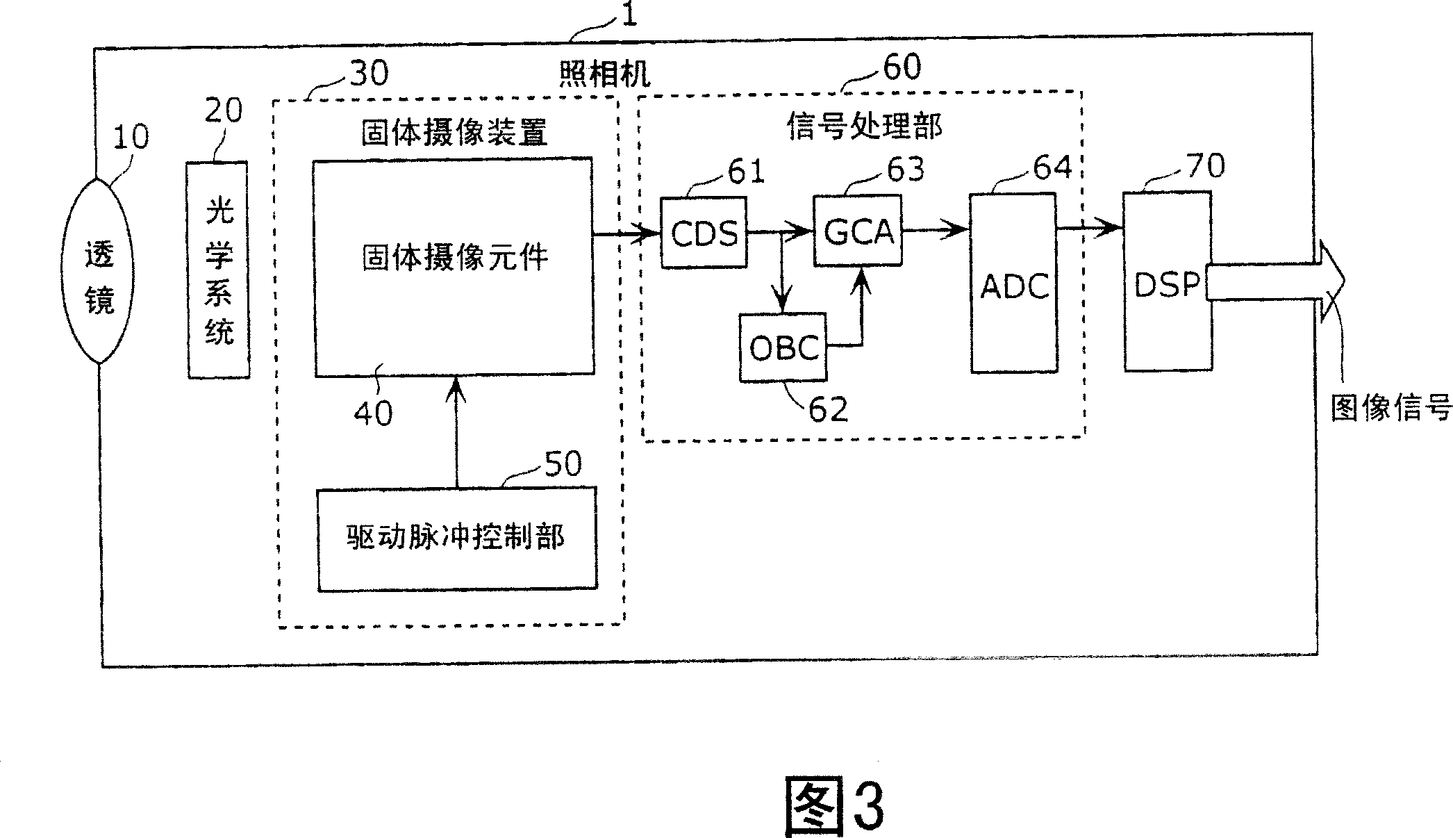
[0056] FIG. 3 is a diagram showing the configuration of a camera using the solid-state imaging device of the present embodiment.

[0057] As shown in Figure 3, the camera 1 has: the lens 10 that makes the optical image of the object imaged on the imaging element; optical systems 20 such as mirrors and mechanical shutters that optically process the optical image passing through the lens 10; A solid-state imaging device 30 ; a signal processing unit 60 ; and a digital signal processor (hereinafter also referred to as “DSP”) 70 and the like.

[0058] The solid-state imaging device 30 has a solid-state imaging element 40 and a drive pulse control unit 50 .

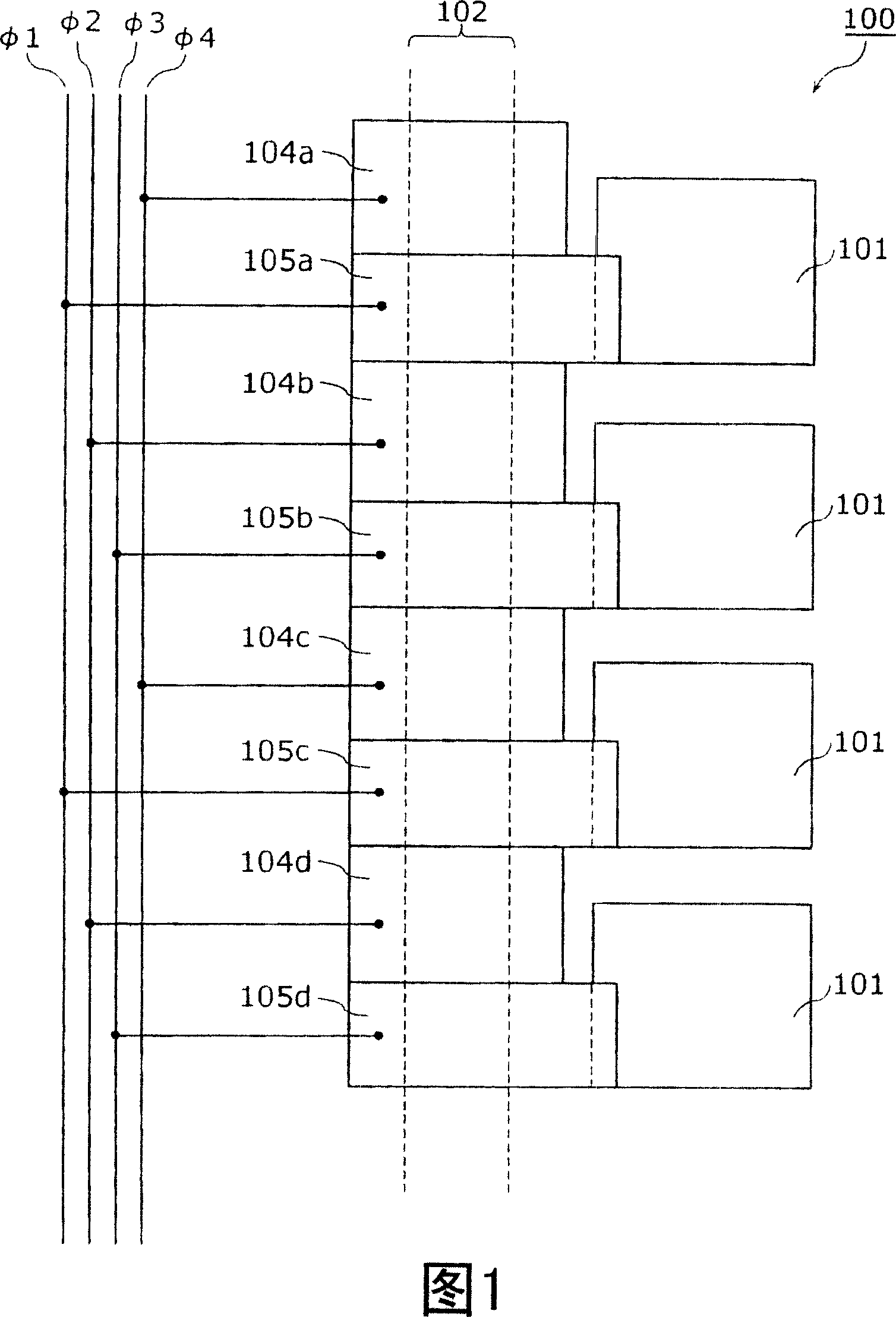
[0059] The solid-state imaging element 40 is realized by a CCD image sensor or the like, and outputs pixel signals corresponding to the amount of received light.

[0060] The drive pulse control unit 50 drives the solid-state imaging device 40 by generating various driving pulses to the solid-state imaging device 40 at variou...

Embodiment approach 2

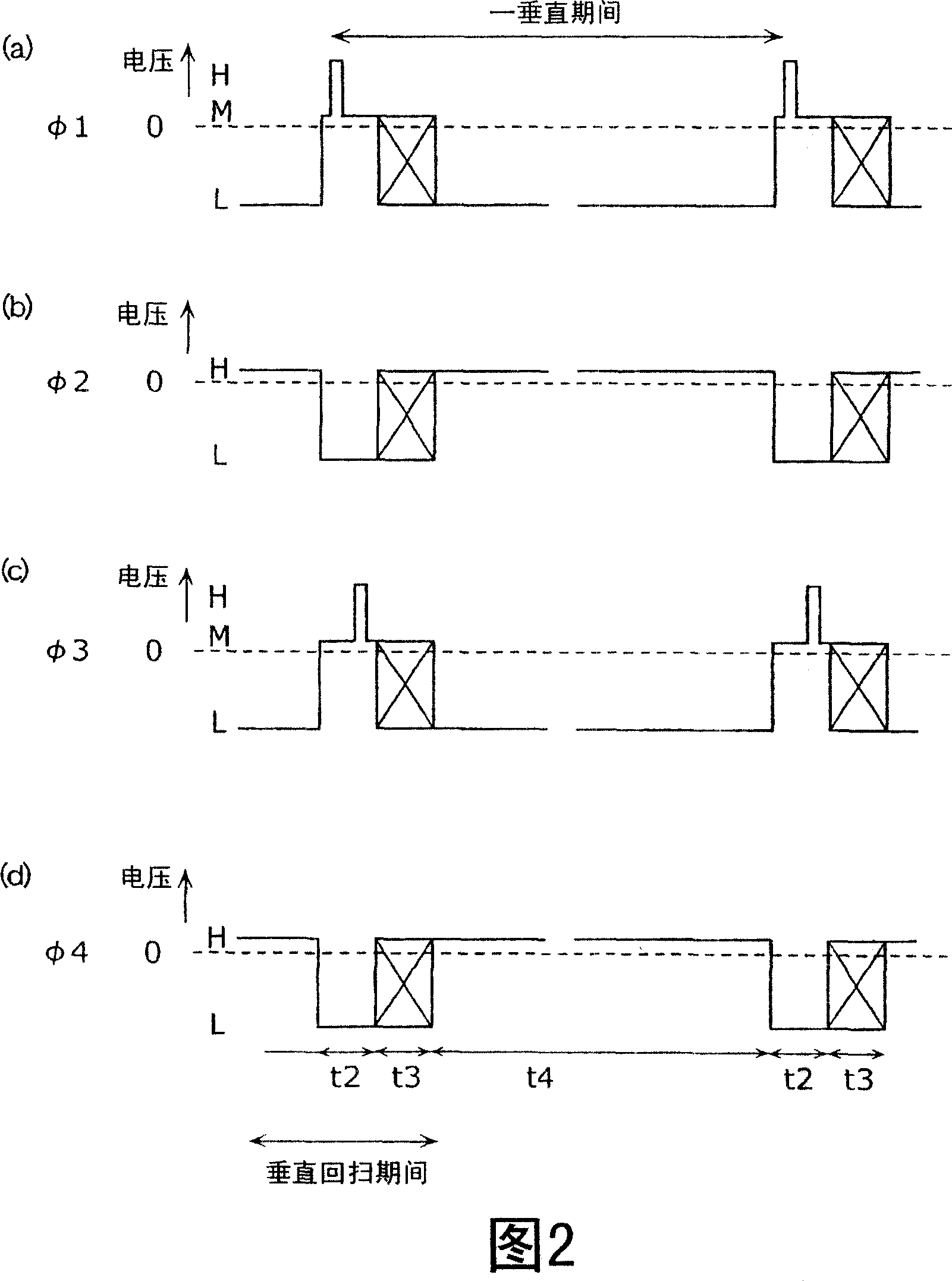
[0147] Next, Embodiment 2 of the present invention will be described. In Embodiment 2, charges are read out to the vertical CCD at a driving timing other than that of Embodiment 1 or at a new driving timing different from that of Embodiment 1. FIG. That is, if the solid-state imaging device can read out the charges accumulated in all the photodiodes to the vertical CCD through N times of readout operations, then when the transfer operation of 1 field or 1 frame is started, as " "Connection action", for the continuous 2N gates composed of N readout gates and N non-readout gates, apply all 2N gates sequentially (that is, staggered timing) to make each gate from a low voltage state A driving pulse that becomes an intermediate voltage state.

[0148] That is, in this embodiment, a function of performing a connection operation during a connection period is added to the solid-state imaging device and the camera described in the first embodiment. Here, the connection period refers ...


PUM


Abstract

The present invention provides a solid-state imaging apparatus which is capable of preventing electric charge from being injected from a semiconductor substrate while electric charge is being accumulated into photodiodes. The solid-state imaging apparatus includes a solid-state imaging device and a driving pulse control unit. The solid-state imaging device includes: a semiconductor substrate, photodiodes which are two-dimensionally formed on the semiconductor substrate, and vertical Charge-coupled devices (CCDs) having at least one arranged read-out gate and non-read-out gate for each of the photodiodes, the read-out gate being for reading out accumulated electric charge from the associated photodiode, and the non-read-out gate being not for reading out accumulated electric charge from the associated photodiode. The driving pulse control unit applies driving pulses sequentially to the respective read-out gates in order to change the read-out gates from stand-by LOW-voltage states to MIDDLE-voltage states, and apply a driving pulse for maintaining a LOW-voltage state of at least one of non-read-out gates adjacent to a last read-out gate in the order of the change among the non-read-out gates, during the change starting with a first read-out gate and ending with the last read-out gate.

Description

technical field [0001] The present invention relates to a solid-state imaging device such as a CCD image sensor and a driving method thereof, and particularly relates to a technique for coping with white spots during long-second accumulation. Background technique [0002] In recent years, solid-state imaging devices have been increased in pixels to 8 million pixels, etc., and it is possible to capture still images like silver salts, or to capture moving images. As a solid-state imaging device with very little so-called smear phenomenon, a frame-interline transfer solid-state imaging device (hereinafter referred to as FITCCD: Frame-Interline Transfer Charge Coupled Device) has been developed. [0003] Next, the configuration of a conventional FITCCD and the driving method of the FITCCD will be described with reference to the drawings. [0004] FIG. 1 is an enlarged view showing a part of the FITCCD. [0005] First, the structure of FITCCD will be described. [0006] In FIG...

Claims


Application Information

Patent Timeline
Patent Type & Authority Applications(China)
IPC IPC(8): H04N3/15H04N5/335H01L27/14H01L27/148H04N25/00
CPCH04N3/1568H04N5/335H01L27/14837H01L27/14843H01L27/14887H04N25/622H04N25/73H04N25/625H01L27/146H04N25/00
Inventor 加藤良章
Owner PANASONIC CORP
Why Eureka
Eureka Blog
Learn More