Micromachined fiber optic sensors

a fiber optic sensor and micromachined technology, applied in the direction of instruments, fluid pressure measurement, fluid pressure measurement by electric/magnetic elements, etc., can solve the problem of limiting the temperature of operation of the sensor, and achieve the effect of reducing costs and adding stability

Inactive Publication Date: 2002-10-31
CINCINNATI UNIV OF
View PDF4 Cites 58 Cited by
  • Summary
  • Abstract
  • Description
  • Claims
  • Application Information

AI Technical Summary

Benefits of technology

0005] This invention uses metal micro-electro-mechanical-systems (MEMS) and micro-optical-electro mechanical systems (MOEMS) including manufacturing components of micro-optic de

Problems solved by technology

Packaging of these sensors usually involves using adhesives

Method used


Image

  • Micromachined fiber optic sensors
  • Micromachined fiber optic sensors
  • Micromachined fiber optic sensors

Examples


example 2

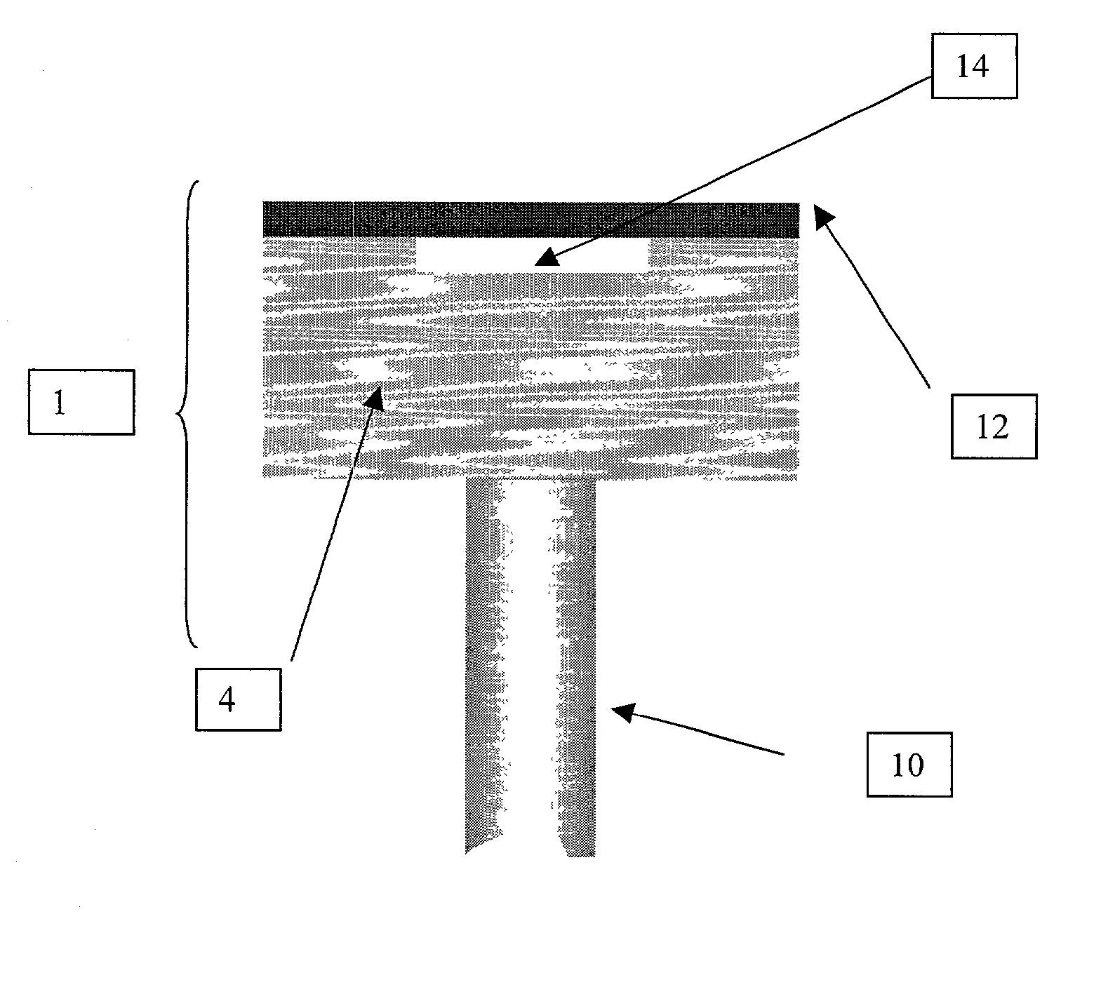
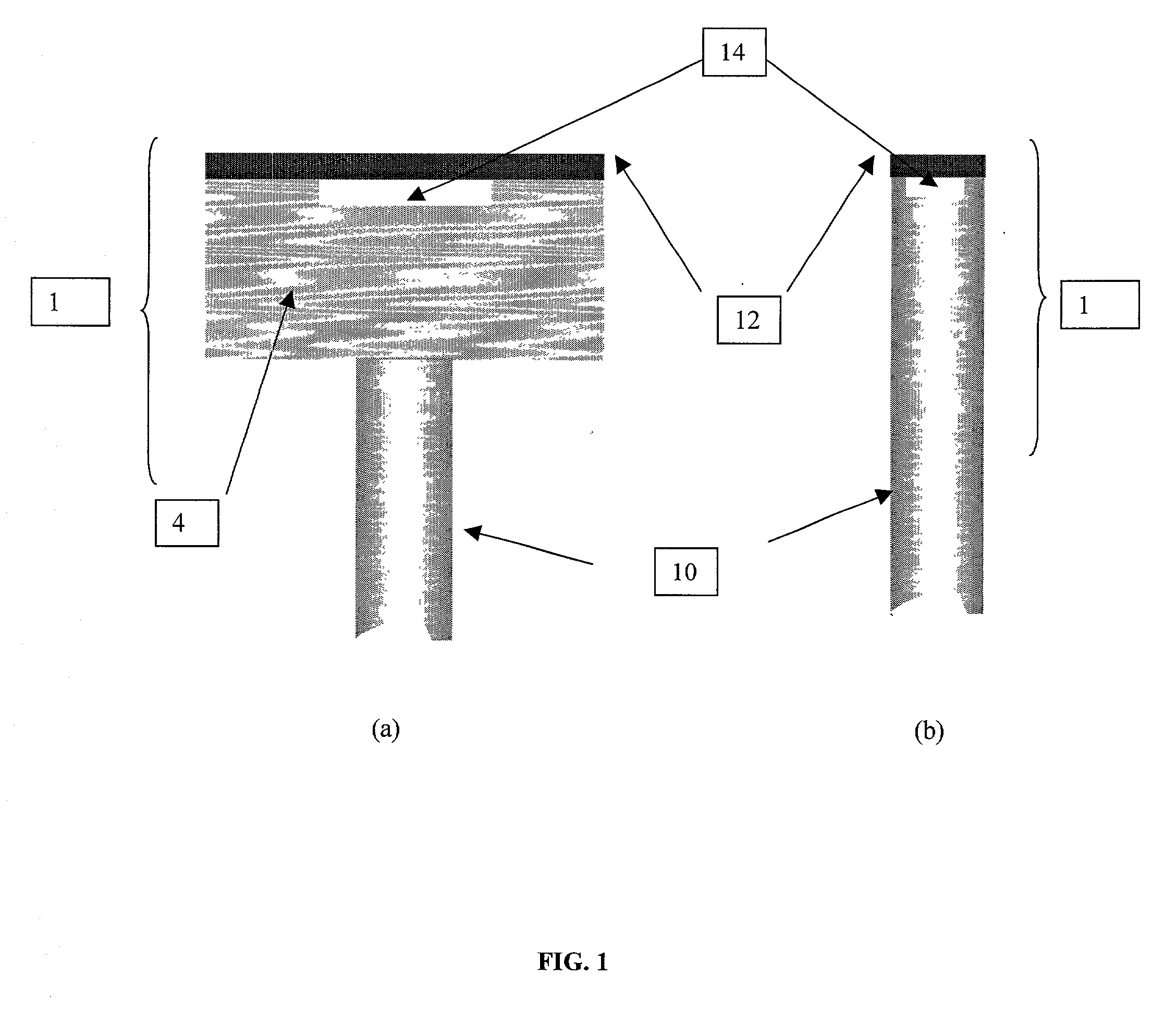
[0068] Temperature Sensor Configuration

[0069] The temperature sensor is achieved by anodically bonding ultra-thin crystalline silicon onto a fiber end face (the figure above). Thin-film based temperature sensors have been realized in a number of ways including sputter-deposited semiconductor [6] and dielectric [7] materials. For effective operation the thickness of the silicon film of these Fabry-Perot interferometer based sensors usually falls within the range of 0.8 .mu.m to 4.3 .mu.m [6]. Greater sensitivity is obtained at the high end of this range; however, film-nonuniformity, and stress have been found to impose an upper thickness limit of about 2 .mu.m for sputter-deposited semiconductors. In this study we used the anodic bonding method to chemically bond ultra-thin crystalline silicon onto fiber end faces; this enables achieving a thicker crystalline silicon layer on the fiber end face. As a result, a higher sensitivity can be expected. Further, the use of crystalline silico...


PUM


Abstract

A novel fiber optic sensor configuration whose diameter is the same as that of the optical fiber on which it is directly fabricated is introduced. A simple MEMS-compatible fabrication process to accomplish micromachining on the fiber end face has been developed and is detailed. This sensor configuration significantly reduces the size of the sensor and makes the packaging simple and adhesive free. The micromachining process of the present invention also provides for the fabrication of arrays of sensors that would provide two dimensional maps with high spatial resolution of at least one of acoustical vibration, mechanical vibration, pressure, temperature, acceleration, electrostatic fields, magnetic fields or combinations thereof.

Description

[0001] This application claims the benefit of U.S. Provisional Patent Application Serial No. 60 / 274,513, filed Mar. 9, 2001, which application is hereby incorporated by reference in its entirety.[0002] The present invention relates to micro-optic sensors used for transmitting pressure sensor signals by optical fibers. More particularly, the invention pertains to fiber optic sensors using silicon structures anodically bonded to the central portion of the fiber end face for detection of at least one of acoustical vibration, mechanical vibration, pressure, temperature, acceleration, electrostatic fields and magnetic fields. The micromachining process of the present invention also provides for the fabrication of arrays of sensors that would provide two dimensional maps with high spatial resolution of at least one of acoustical vibration, mechanical vibration, pressure, temperature, acceleration, an electrostatic field magnetic field or combinations thereof.[0003] Optical fibers have bee...

Claims


Application Information

Patent Timeline
IPC IPC(8): G01D5/26G01L9/00G02B6/26
CPCG01D5/268G02B6/262G01L9/0079
Inventor BOYD, JOSEPH T.ABEYSINGHE, DON C.DASGUPTA, SAMHITAJACKSON, HOWARD E.
Owner CINCINNATI UNIV OF
Why Eureka
Try Eureka