
Eureka
For R&D, Eureka makes reading and utilizing patents & technical documents easy.
Eureka AIR
Designed for self-driven R&D workflows. Generate viable solutions, solve complex R&D challenges, empower your innovation with AI.

Eureka Materials
Designed for material experts only. Revolutionize your material R&D, from search, analyze, to developing new materials.

TechResearch
Generate reliable direction feasibility study reports for your R&D in just a few steps.

TechSeek
Discover and master advanced knowledge NOW. Basics, ideas, possibilities, all at once.

TechMind
As an expert in R&D Theories, TechMind can generates customized viable solutions instantly.

TechRisk
Analyze your overall solution with one click, know your potential R&D risks in advance.

TechMonitor
Get weekly tech updates, stay abreast of the latest tech innovations and key insights.
Method for manufacturing thin-film transistor and semiconductor element
A technology of a thin film transistor and a manufacturing method, which is applied to the manufacturing field of thin film transistors, can solve the problems of high mask cost and difficulty in reducing manufacturing cost, and achieve the effects of reducing mask cost and avoiding alignment errors.
- Summary
- Abstract
- Description
- Claims
- Application Information
AI Technical Summary
Problems solved by technology
Method used
Image

Examples
no. 1 example
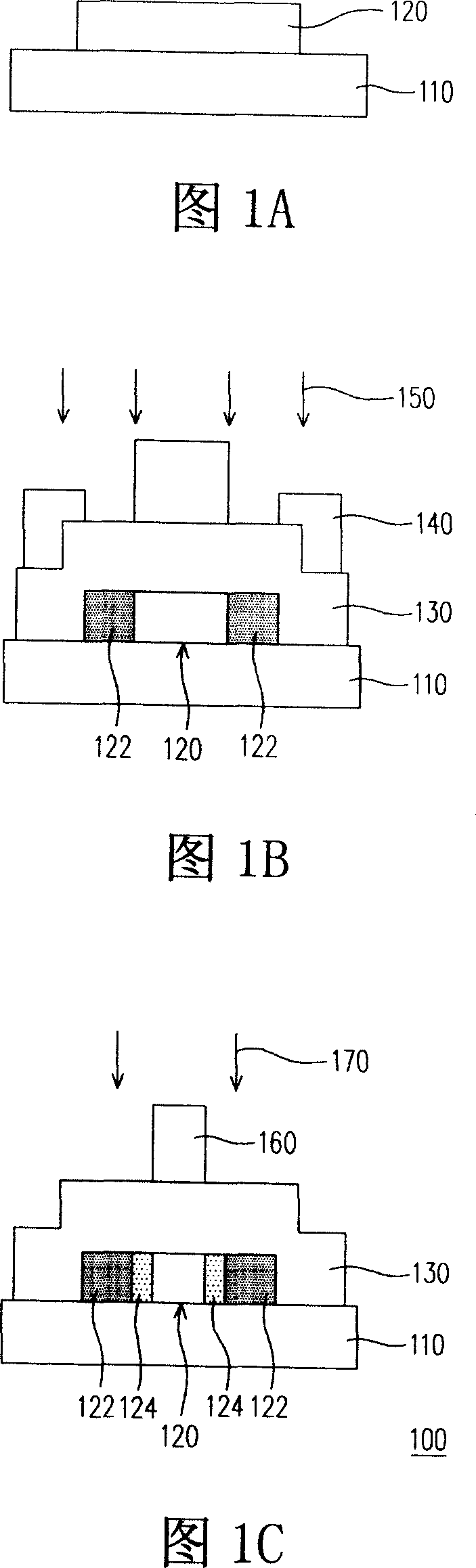
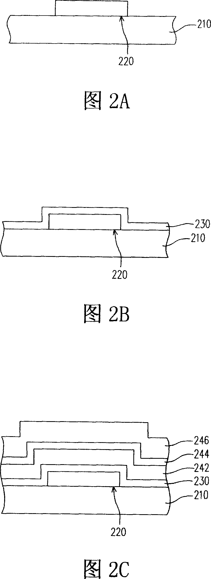
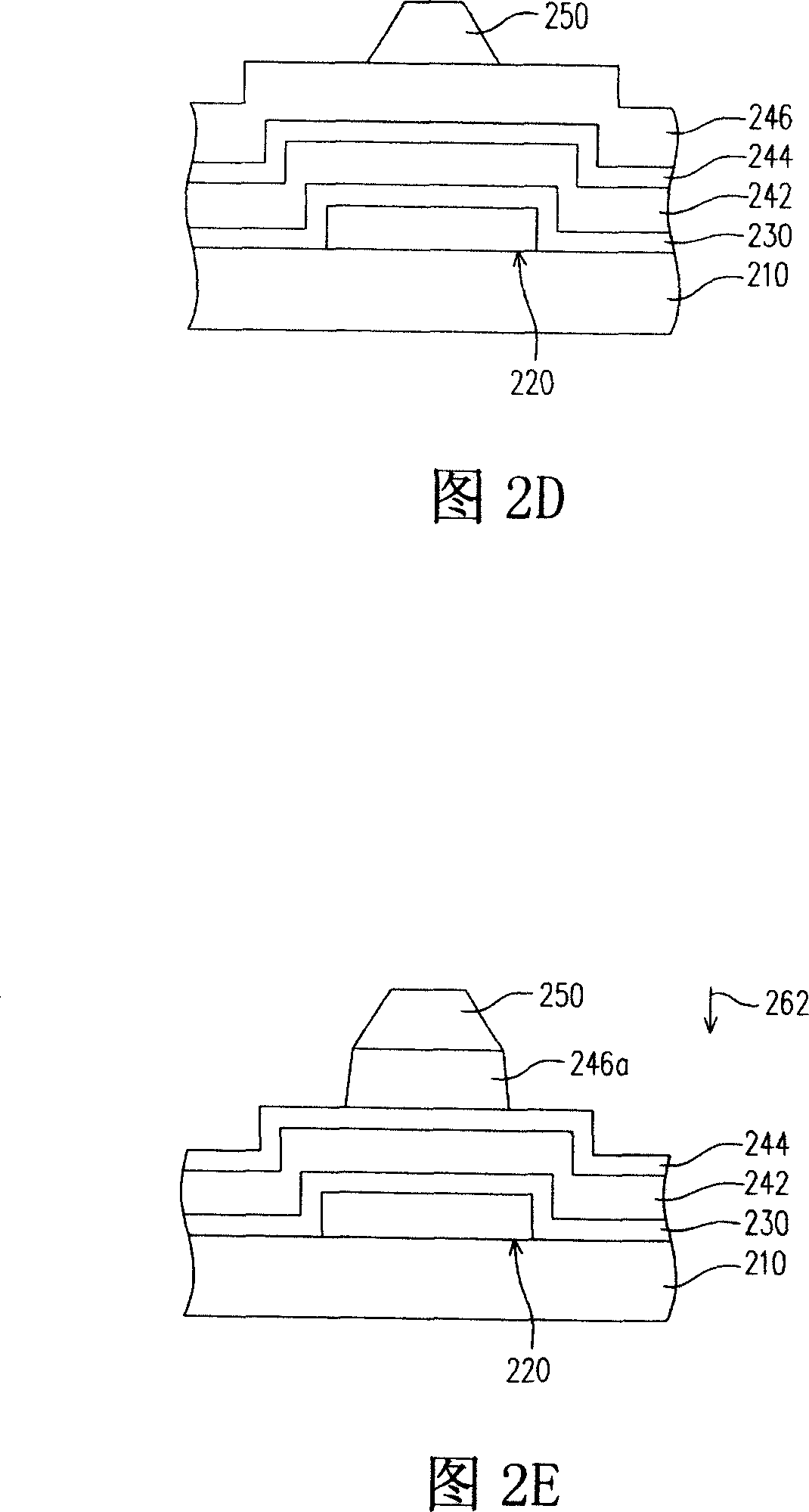
[0060] 2A to 2K are schematic cross-sectional schematic diagrams showing the steps of the manufacturing method of the thin film transistor according to a preferred embodiment of the present invention, please refer to FIG. 2A to FIG. 2K together.
[0061] Referring to FIG. 2A , a patterned polysilicon layer 220 is formed on a substrate 210 . In one embodiment, the patterned polysilicon layer 220 is formed by the following steps, for example. First, an amorphous silicon layer (not shown) is formed on the substrate 210 . Then, an annealing process is performed to form a polysilicon layer (not shown) from the amorphous silicon layer. The annealing process is, for example, an excimer laser annealing process (Excimer Laser Annealing, ELA). Then, a photoresist layer (not shown) is formed on the polysilicon layer, and the photoresist layer is patterned using a first mask (not shown) to form a patterned photoresist layer (not shown) . Afterwards, the polysilicon layer is etched usin...
no. 2 example
[0081] The present invention also proposes a method for manufacturing a semiconductor element, most of the manufacturing steps of which are similar to the method for manufacturing the thin film transistor of the first embodiment, and the same steps will not be repeated. Here, only partial steps are shown as shown in FIGS. 3A to 3D .
[0082] 3A to 3D are schematic cross-sectional views showing partial steps of a method for fabricating a semiconductor device according to a preferred embodiment of the present invention. Please refer to FIG. 3A to FIG. 3D together.
[0083] Firstly, the steps described in FIGS. 2A to 2K are performed on the substrate 210 to fabricate the thin film transistor 200 . The TFT 200 is composed of a substrate 210, a patterned polysilicon layer 220, a gate dielectric layer 230, a first gate layer 242b and a second gate layer 244b. Wherein, a source / drain region 220 a , a channel region 220 b , and a lightly doped source / drain region 220 c are formed in...
PUM
 Abstract
Description
Claims
Application Information
 - R&D Engineer
- R&D Manager
- IP Professional
- Industry Leading Data Capabilities
- Powerful AI technology
- Patent DNA Extraction
Browse by: Latest US Patents, China's latest patents, Technical Efficacy Thesaurus, Application Domain, Technology Topic, Popular Technical Reports.
© 2024 PatSnap. All rights reserved.Legal|Privacy policy|Modern Slavery Act Transparency Statement|Sitemap|About US| Contact US: help@patsnap.com