A method for preparing the nano-electrode with the negative electronic erosion-resisting agent

A nano-electrode and resist technology, applied in the field of nano-electrode preparation, can solve the problems of optical lithography resolution difficult to reach nanoscale resolution, low efficiency, single electrode material, etc.

Inactive Publication Date: 2007-08-15
INST OF MICROELECTRONICS CHINESE ACAD OF SCI
View PDF3 Cites 11 Cited by
  • Summary
  • Abstract
  • Description
  • Claims
  • Application Information

AI Technical Summary

Problems solved by technology

The Chinese invention patent with application number 200410010181.2 uses an atomic force microscope (AFM) to etch nanowires combined with chemical methods to prepare silver nanoelectrodes, which has the disadvantages of low efficiency and incapable of large-scale production
The Chinese invention patent with application number 99116576.4 uses flame melting and etching methods to prepare carbon fiber nano-electrodes, the electrode material is single, and it is only used in the biological field
Due to its high efficiency, optical lithography is currently the mainstream technology for making electrodes, but the resolution of optical lithography is limited by the exposure wavelength and it is difficult to achieve nanoscale resolution.

Method used


Image

  • A method for preparing the nano-electrode with the negative electronic erosion-resisting agent
  • A method for preparing the nano-electrode with the negative electronic erosion-resisting agent
  • A method for preparing the nano-electrode with the negative electronic erosion-resisting agent

Examples


specific Embodiment

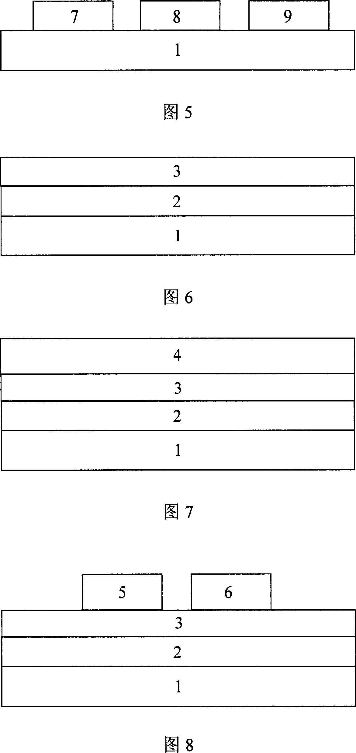
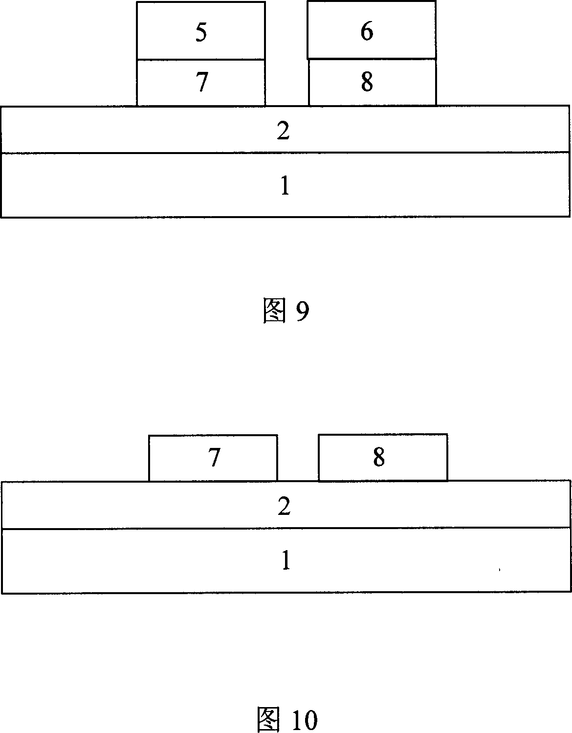
[0029] Taking the use of SOI substrate, SAL601 chemically amplified negative electronic resist, and ICP etching as an example, the detailed process and steps of the present invention are further described in conjunction with the accompanying drawings, wherein:

[0030] As shown in Figure 6, a p-type, (111) crystal-oriented SOI substrate is used, and the SOI substrate is composed of a silicon base 1, a 375nm-thick buried oxide layer 2, and a 50nm-thick top layer silicon 3 from bottom to top. constitute. P 31+ ions, the implantation energy is 20keV, and the implantation dose is 1×10 15 cm -2 , then at N 2 Rapid annealing at 1200° C. for 10 seconds in an atmosphere improves the conductivity of the top layer silicon 3 .

[0031] As shown in FIG. 7 , SAL601 chemically amplified negative electronic resist 4 was coated on the SOI substrate with a coater, the coating speed was 3000 rpm, and the coating time was 60 seconds. Then pre-bake at 110° C. for 3 minutes with a hot plate. ...


PUM


Abstract

The preparation method for nano electrode comprises: growing well-conductive metal or semiconductor layer; using EBL to obtain a couple or group negative electronic anti-corrosive agent, and coating the agent; first baking; with electron beam to direct expose; developing, fixing, etching, and stripping the photoresist. The product has 20-100nm space and fit to wide application. This invention is simple and reliable, and compatible with traditional CMOS technology.

Description

technical field [0001] The invention belongs to the technical field of nano processing, in particular to a preparation method of a nano electrode. Background technique [0002] For more than half a century, semiconductor integrated circuits with CMOS as the mainstream technology have been developing rapidly following "Moore's Law". Nanoelectronic devices with new principles, such as various quantum dot devices, nanowires, nanotube devices, and single-electron devices, have become research hotspots. In the manufacture of these nanoelectronic devices, the manufacture of nanoelectrodes with small size, good conductivity and nanoscale gaps is a key and difficult point. [0003] The Chinese invention patent with application number 200410095163.9 mainly uses chemical methods combined with the use of polymer materials to prepare electrodes, but this electrode has not reached the nanometer scale. The Chinese invention patent with the application number 200410010181.2 uses an atomi...

Claims


Application Information

Patent Timeline
Patent Type & Authority Applications(China)
IPC IPC(8): H01L21/283G03F7/00
Inventor 龙世兵刘明陈宝钦
Owner INST OF MICROELECTRONICS CHINESE ACAD OF SCI
Why Eureka
Try Eureka