A compound bar, bar source self-separating VDMOS, 1GBT power unit and its making technology

A power device and manufacturing process technology, which is applied in the field of composite gate, gate-derived isolation VDMOS, IGBT power devices and their manufacturing process, can solve problems such as poor economy and practicability, affecting working life, and complex product costs, and achieve product The effect of easy quality assurance, simplified manufacturing process, and enhanced yield

Inactive Publication Date: 2007-08-15
上海富华微电子有限公司 +1
View PDF0 Cites 13 Cited by
  • Summary
  • Abstract
  • Description
  • Claims
  • Application Information

AI Technical Summary

Problems solved by technology

The structural form of this double isolation layer makes the N+ area of ​​the VDMOS and IGBT power devices made in this way larger, and makes the emission area of ​​the parasitic NPN tube larger, and the structural form of this isolation layer , due to the process relationship, it is easy to short-circuit the gate and the source and affect the working life. In addition to causing poor reliability of the VDMOS and IGBT power devices, the production process is complex and the product cost remains high, so the economical and poor practicality

Method used


Image

  • A compound bar, bar source self-separating VDMOS, 1GBT power unit and its making technology
  • A compound bar, bar source self-separating VDMOS, 1GBT power unit and its making technology
  • A compound bar, bar source self-separating VDMOS, 1GBT power unit and its making technology

Examples


Embodiment Construction

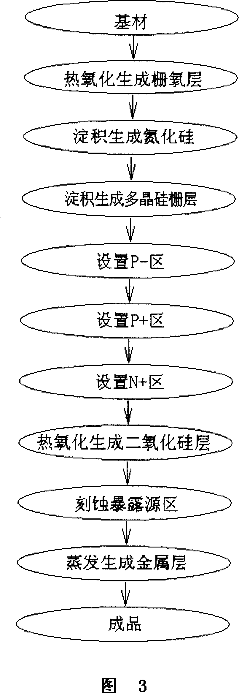
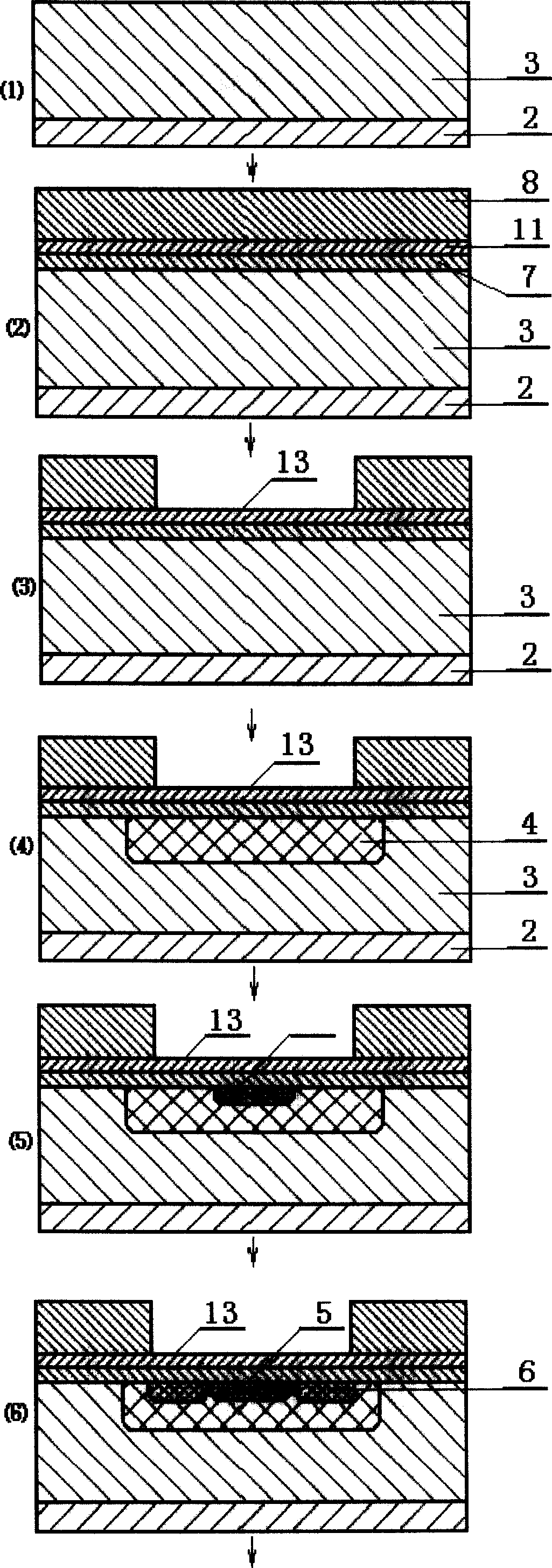
[0033] The present invention will be further described below in conjunction with the accompanying drawings and typical embodiments.

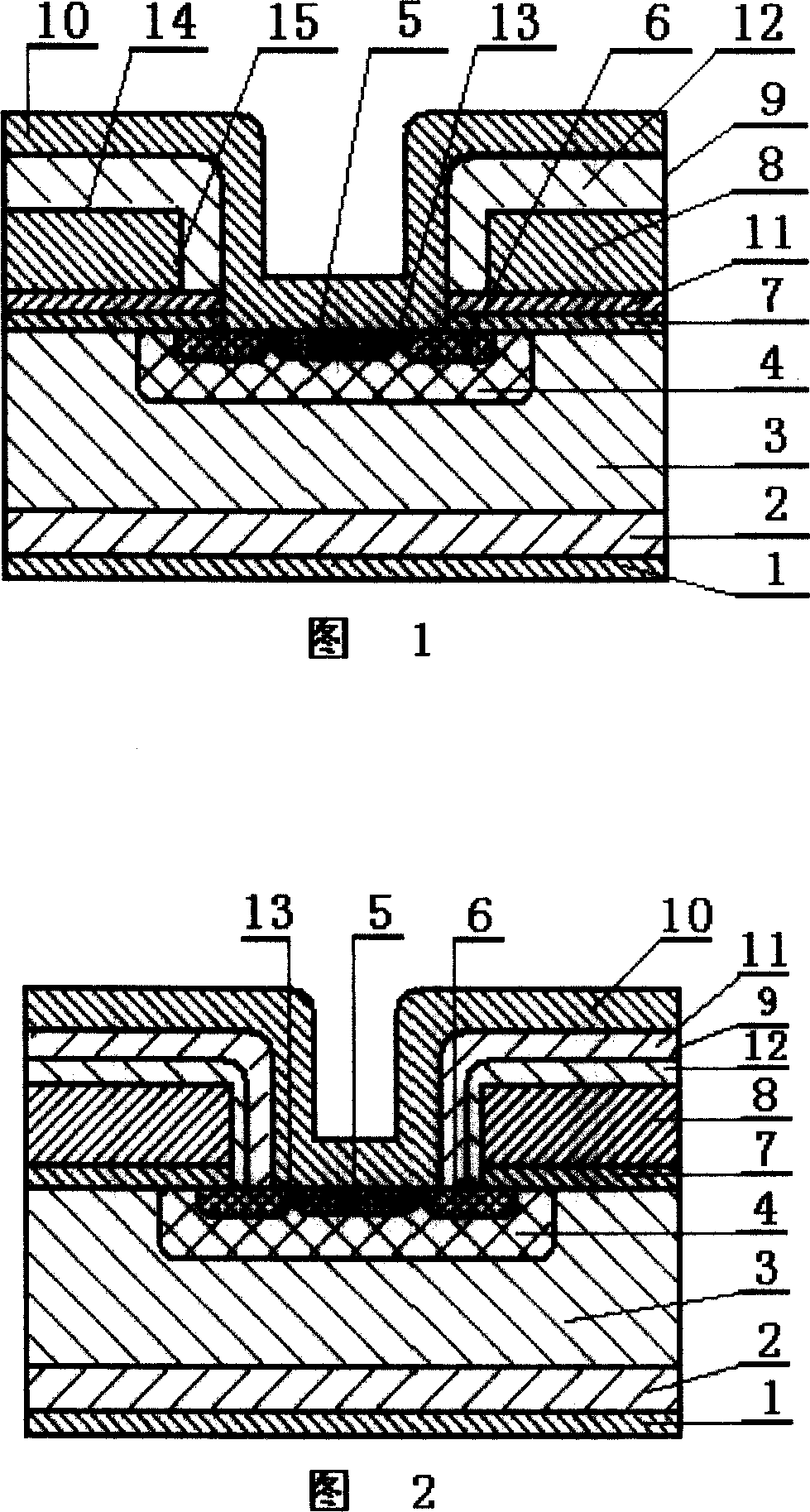
[0034] In Fig. 1 and Fig. 2, composite gate of the present invention, gate originates from isolation VDMOS, IGBT power device mainly is by metal bottom layer 1, N+ substrate layer (in IGBT is P+ substrate layer) 2, N- epitaxial layer 3, P -zone 4, P+ zone 5, N+ zone 6, thermally oxidized SiO 2It consists of a gate oxide layer 7, a polysilicon gate layer 8, a source gate isolation layer 9 and a metal surface layer 10. The metal surface layer 10 acts as the source, the metal bottom layer 1 acts as the drain, and the polysilicon gate layer 8 acts as the gate. The source region consists of the P-region 4 located in the deep layer, the P+ region 5 located in the middle of the surface layer, and the ring-shaped N+ region located on the periphery of the P+ region 5. 6 composition. It is characterized in that thermal oxide SiO is provided between the ...


PUM


Abstract

The invention relates to VDMOS and IGBT power device with composite grid and self-isolated grid-source. Wherein, it sets a thermal-oxidized SiO2 grid between source and multicrystal Si grid, and adds a Si3N4 layer to form a composite grid together with last grid to increase grid yield. Compared with prior art, this invention increase can fast shield grid window and generate only -very-thin oxidation layer to simplify manufacture technology, and needs low cost.

Description

technical field [0001] The invention relates to the manufacturing process technology of semiconductor devices in the field of microelectronics technology, in particular to a compound gate, gate-derived isolation VDMOS, IGBT power device and its manufacturing process. Background technique [0002] Existing VDMOS and IGBT power devices are mainly composed of metal bottom layer, N+ substrate, silicon N- epitaxial layer, P- region, P+ region, N+ region, thermal oxide SiO 2 Gate oxide layer, polysilicon layer, SiO 2 Deposition layer, phosphosilicate glass PSG deposition layer and metal surface layer. The metal surface acts as the source, the metal bottom layer acts as the drain, the polysilicon layer acts as the gate, the phosphosilicate glass PSG layer and LPCVD SiO 2 The layer acts as an isolation layer, and the source region consists of a P-region in the deep layer, a P+ region in the middle, and an annular N+ region on the periphery of the P+ region. [0003] Its manufactu...

Claims


Application Information

Patent Timeline
Patent Type & Authority Applications(China)
IPC IPC(8): H01L29/78H01L29/739H01L21/336H01L21/331
Inventor 邵光平
Owner 上海富华微电子有限公司
Why Eureka
Try Eureka