Chip with light protection layer

A light protection and chip technology, applied in electrical components, electrical solid devices, circuits, etc., can solve the problems of large total chip thickness, high cost, erosion, etc., and achieve the effect of high reflectivity and good protection

Inactive Publication Date: 2007-08-29
NXP BV
View PDF1 Cites 2 Cited by
  • Summary
  • Abstract
  • Description
  • Claims
  • Application Information

AI Technical Summary

Problems solved by technology

Furthermore, such epoxy coatings have a thickness that is not suitable for realizing very thin chips, such as those used in radio frequency identification applications (RFID applications), since the overall thickness of the chip would be too large due to the epoxy coating
Furthermore, there is a risk of erosion, since the added colorants in many cases have a relatively high proportion of ions
To eliminate this erosion problem, ultrapure "colorants" can be used, but due to the complex purification process required for their manufacture, these ultrapure "colorants" are very expensive
In addition, there is a problem that, in most cases, it is not possible to incorporate the photoprotective layer because the materials and methods (for example, wet chemical methods) commonly used to manufacture the photoprotective layer have the risk of introducing contamination during the chip production process. Coating is integrated in the chip production process but is performed separately from the actual manufacturing process of the chip
[0006] However, in the case of the known chip, the disadvantage has been demonstrated that the conductive material used to create the photoprotective layer promotes the generation of parasitic capacitances, which constitute a risk of impairing the mode of operation of the chip

Method used


Image

  • Chip with light protection layer
  • Chip with light protection layer

Examples


Embodiment Construction

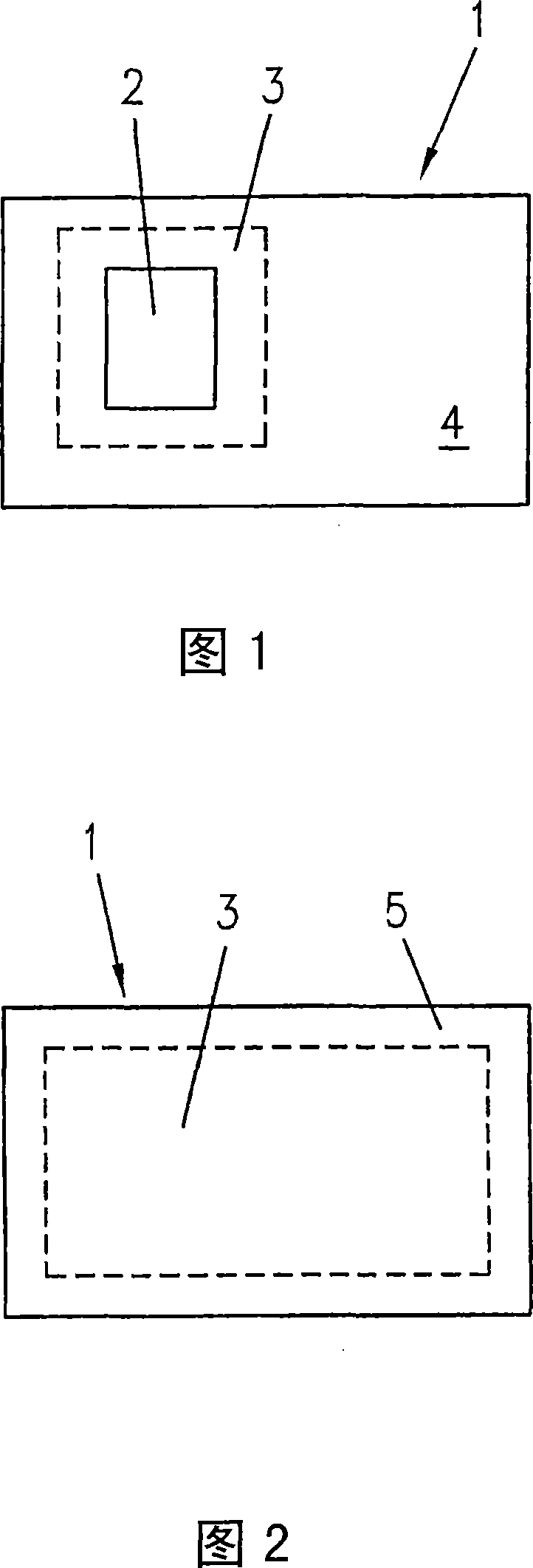
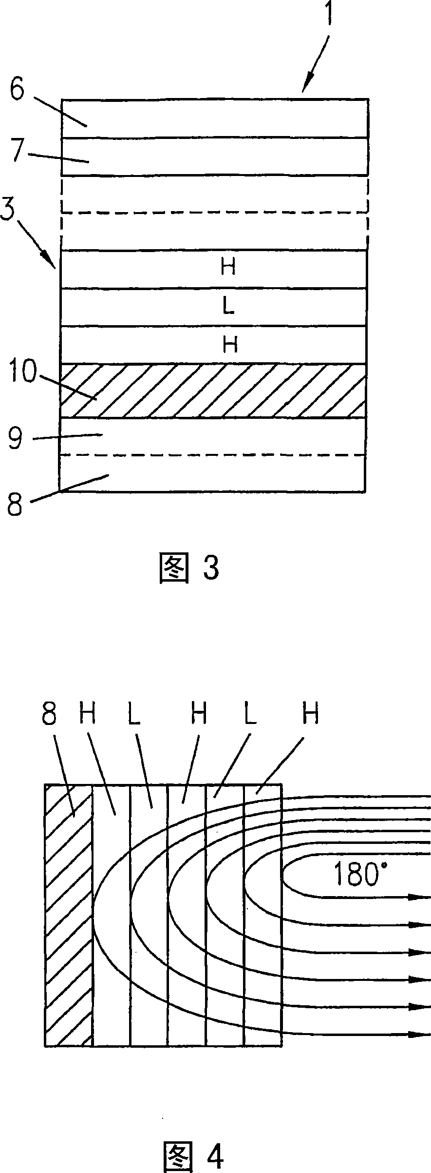
[0022] FIG. 1 shows a chip 1 according to the invention, with an integrated circuit 2 . In principle, several integrated circuits 2 can be realized on the chip 1 independently of one another. The integrated circuit 2 is implemented on a first side 4 of the chip 1 , commonly referred to as the "active side", and is protected from the effects of light by a dielectric mirror coating 3 applied to the surface of the chip 1 .

[0023] From the literature, a relatively wide variety of dielectric mirror coatings have been known to those skilled in the art for a considerable time. All dielectric mirror coatings generally share the fact that they consist of two or more dielectric λ / 4 layers, the adjacent dielectric layers having different refractive indices. Regarding dielectric mirror coatings, the reader is referred to Matt Young, "Optik Laser, Welleleiter", Springer, 1997; pp 160-161 as an example. Despite this fact, experts in the field of integrated circuit chips have never sugge...


PUM


Abstract

In the case of a chip (1) having an integrated circuit (2), a dielectric mirror coating (3) having at least two dielectric layers (6, 7,..... H, L, H) is applied as light protection means for the at least one integrated circuit (2) on at least one portion of the surface of the chip (1).

Description

technical field [0001] The invention relates to a chip with at least one integrated circuit and with a light protection device for the at least one integrated circuit. [0002] The invention also relates to a method for producing a chip with at least one integrated circuit and with a light protection device for the at least one integrated circuit. Background technique [0003] Because the semiconductors used in chips are usually highly light-sensitive in terms of the photoelectric effect, it is often necessary to provide light protection for the chip. [0004] Due to the semiconductor material used, the problem with the chip is that even small amounts of light in the UV, VIS and IR range incident on its unprotected surface can seriously affect or actually prevent the chip's performance due to the generated charges. Function. Also, specific security circuits (for example, those used in security chips) may be deliberately disabled by irradiation of light of a specific wavele...

Claims


Application Information

Patent Timeline
Patent Type & Authority Applications(China)
IPC IPC(8): H01L23/552
CPCH01L2924/0002H01L23/552H01L23/573H01L2924/00
Inventor 克里斯蒂安·岑茨
Owner NXP BV
Why Eureka
Try Eureka