

Enclosed infrared heating device for semiconductor chip
A heating device, infrared technology, applied in electric heating device, semiconductor/solid state device manufacturing, ohmic resistance heating and other directions, can solve the problems of low heating efficiency, no cooling of the lamp, affecting the life of the lamp, etc., to achieve good cooling effect, The effect of improving heating efficiency
Inactive Publication Date: 2007-09-19
48TH RES INST OF CHINA ELECTRONICS TECH GROUP CORP
View PDF0 Cites 9 Cited by
- Summary
- Abstract
- Description
- Claims
- Application Information
AI Technical Summary
Problems solved by technology
[0002] Wafer heating on the semiconductor process line generally adopts non-contact radiation heating. In traditional heating devices, the heating lamp directly faces the wafer for heating. The lamp is not cooled. Due to poor heat dissipation, the temperature of the lamp holder and the surface of the lamp The rise is very high, causing high-temperature volatiles to affect the cleanliness of the system. The high temperature on the surface of the lamp tube softens the glass bulb of the lamp tube, which affects the life of the lamp tube, and the heating efficiency is not high.
Method used
View moreImage
Smart ImageViewing Examples

Examples
Embodiment Construction
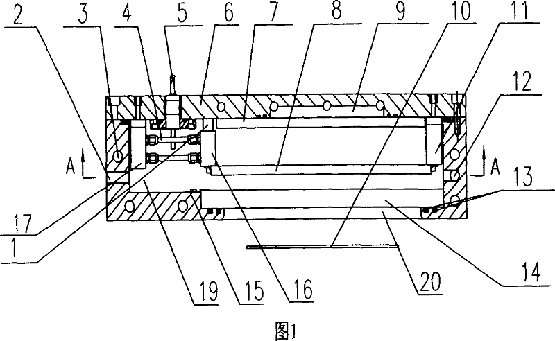
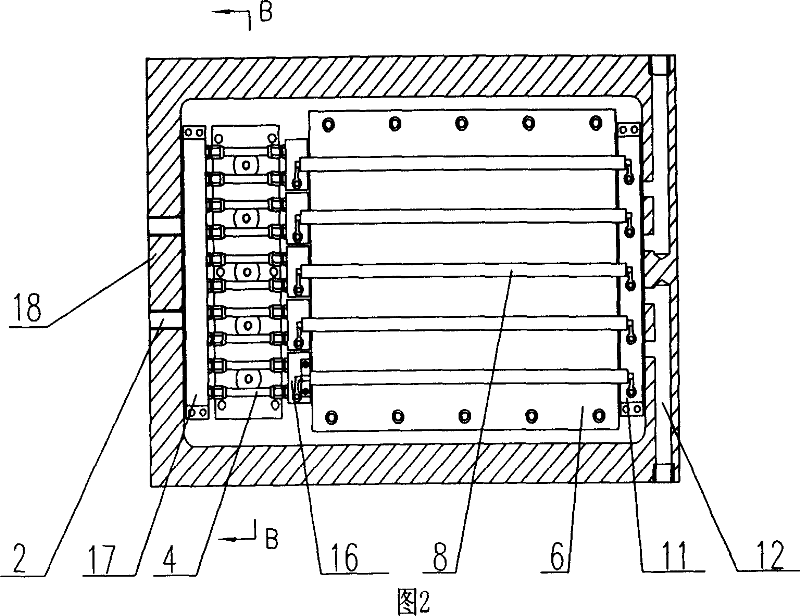
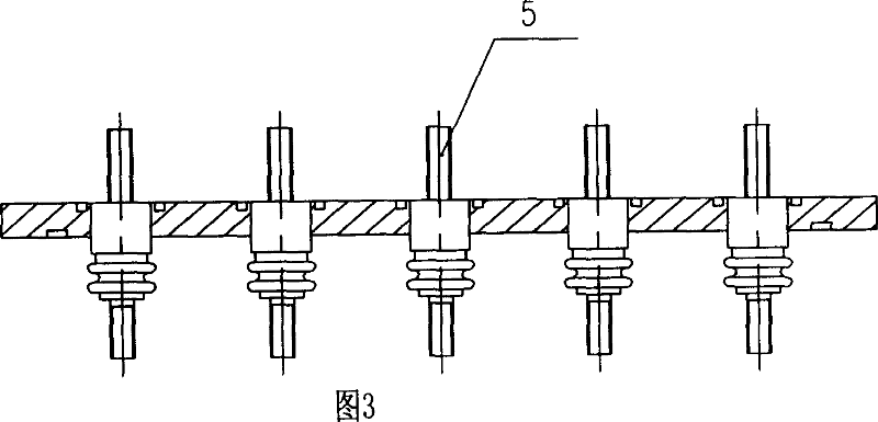
[0024] According to the accompanying drawings and the device of the present invention with the above-mentioned structure, there are five heating lamp tubes 8, five corresponding lamp tube holders 16, the device heating power is 25KW, and the heating temperature is the highest 800°C; the transmission glass 14 shown in Fig. 1 is made of high-purity Quartz glass, a high-temperature-resistant sealing ring 13 is installed between it and the housing 18, and is fixed with a pressing plate 15. The reflecting plate 7 is made of brass plate, and the reflecting surface is plated with gold; Vacuum isolated power supply.
Login to View More PUM
 Abstract
The invention provides a closed infrared heater for semiconductor wafer, which includes an infrared generating chamber disposed at the inner of a shell having seal cover, a transmission window seal by transmission glass is arranged on one side of the shell, wherein, the two ends of the chamber respectively has lamp holders for mounting at least two lamps, and a reflection plate is disposed on one side of the lamps, and each lamp holder is mounted on the cover plate by insulation pillars and is connected to the power supply base, sub water inlets and sub water back ports arranged at the two ends of cooling water channel of each lamp holder are respectively connected to corresponding water back ports and water inlets of the water diversion bus, cooling water channel of the water diversion bus is connected to the same of the cover plate, and some cooling water channels of the shell are connected to the same of the cover plate, and air inlets and air outlets are respectively arranged on both sides of the shell. The invention is fit for radiation heating the movable wafer or fixed wafer of the semiconductor device, and has no pollution, can work in vacuum condition, and is fit for heating material such as silicon wafer which requires high cleanliness.
Description
technical field [0001] The present invention is semiconductor material processing equipment, and further refers to a closed infrared heating device for heating semiconductor wafers. Background technique [0002] Wafer heating on the semiconductor process line generally adopts non-contact radiation heating. In traditional heating devices, the heating lamp directly faces the wafer for heating. The lamp is not cooled. Due to poor heat dissipation, the temperature of the lamp holder and the surface of the lamp The rise is very high, causing high-temperature volatiles to affect the cleanliness of the system. The high temperature on the surface of the lamp tube softens the glass bulb of the lamp tube, which affects the life of the lamp tube, and the heating efficiency is not high. As the cleanliness requirements of semiconductor manufacturing process lines are getting higher and higher, wafer heating requires non-polluting heating methods and heating devices with high thermal effi...
Claims
Login to View More Application Information
Patent Timeline
 Patent Type & AuthorityApplications(China)
IPC IPC(8): H01L21/00H05B3/00
Inventor贾京英刘咸成王学仕
Owner48TH RES INST OF CHINA ELECTRONICS TECH GROUP CORP