Semiconductor integrated circuit device

一种集成电路、半导体的技术,应用在半导体集成电路器件领域,能够解决未参考电流、未公开TDDB电场强度与布局关系等问题,达到改善ESD耐压的效果

Inactive Publication Date: 2007-09-19
NEC ELECTRONICS CORP
View PDF2 Cites 10 Cited by
  • Summary
  • Abstract
  • Description
  • Claims
  • Application Information

AI Technical Summary

Problems solved by technology

Japanese Unexamined Patent Publication No. 2005-129902 discloses how to improve TDDB life from the aspects of manufacturing process and structure, but does not disclose the relationship between the electric field strength and layout of TDDB life
Japanese Unexamined Patent Publication No. 2005-223245 discloses the ESD protection element formed under the pad, but does not refer to the relationship between the current flowing through the line and the low dielectric constant film when the ESD protection element operates

Method used


Image

  • Semiconductor integrated circuit device
  • Semiconductor integrated circuit device
  • Semiconductor integrated circuit device

Examples


no. 1 example

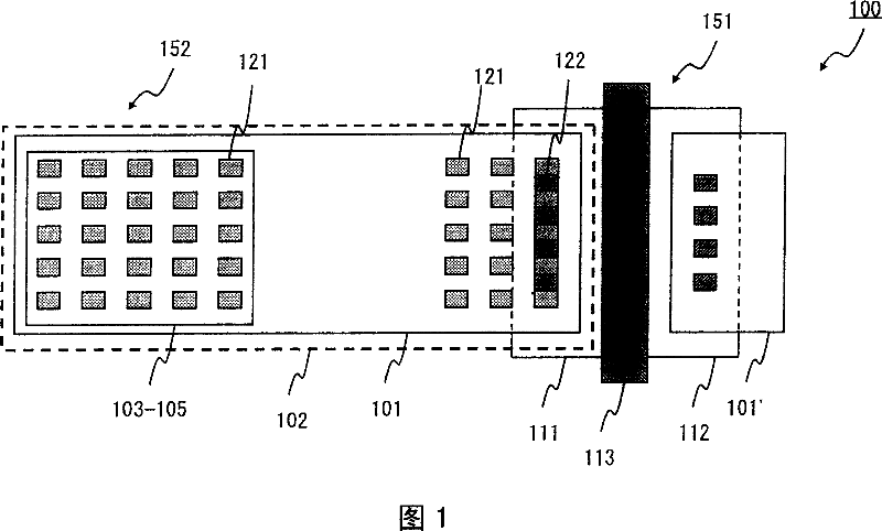
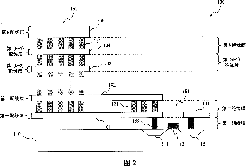
[0038] First, a semiconductor integrated circuit device according to a first embodiment of the present invention will be described. A low dielectric constant film is used for the insulating layer of the semiconductor integrated circuit device of this embodiment. In the semiconductor integrated circuit device of the present embodiment, metal lines extending toward the protection element are formed in a plurality of wiring layers.

[0039] The configuration of the semiconductor integrated circuit device of the present embodiment will be described below with reference to FIGS. 1 and 2 . 1 and 2 illustrate structures of input / output pads and protection elements of the semiconductor integrated circuit device 100 . 1 is a plan view of a semiconductor integrated circuit device 100, and FIG. 2 is a cross-sectional view of the semiconductor integrated circuit device 100 shown in FIG.

[0040] As shown in FIG. 2 , the semiconductor integrated circuit device 100 includes a protection e...

no. 2 example

[0063] Next, a semiconductor integrated circuit device according to a second embodiment of the present invention is described. A low dielectric constant film is used for the semiconductor integrated circuit device of this embodiment. Furthermore, the semiconductor integrated circuit device of the present embodiment has two power supply lines formed in different wiring layers.

[0064] The configuration of the semiconductor integrated circuit device of the present embodiment will be described below with reference to FIGS. 5A and 5B . 5A and 5B show the structure of the power supply line of the semiconductor integrated circuit device 200. As shown in FIG. FIG. 5A is a plan view of the semiconductor integrated circuit device 200 . FIG. 5B is a cross-sectional view of the semiconductor integrated circuit device 200 in FIG. 5A.

[0065] The semiconductor integrated circuit device 200 has a Vcc line 201 for supplying a power supply potential and a GND line 202 for supplying a gro...

no. 3 example

[0070] Next, a semiconductor integrated circuit device according to a third embodiment of the present invention is described. In the semiconductor integrated circuit device of this embodiment, a low dielectric constant film is used for the insulating layer. Furthermore, the semiconductor integrated circuit device of the present embodiment is characterized in that the source potential line and the drain potential line of the MOSFET are formed in different wiring layers.

[0071] The configuration of the semiconductor integrated circuit device 300 of the present embodiment will be described below with reference to FIGS. 6 and 7 . 6 and 7 show the structure of MOSFET and source / drain potential lines. FIG. 6 is a plan view of the semiconductor integrated circuit device 300 . FIG. 7 is a cross-sectional view of the semiconductor integrated circuit device 300 in FIG. 6. Referring to FIG.

[0072] As shown in FIG. 7 , the semiconductor integrated circuit device 300 includes a MOSF...


PUM


Abstract

A semiconductor integrated circuit device according to an embodiment of the invention includes: a protective element formed on a semiconductor substrate; and a plurality of wiring layers composed of insulating layers including a layer that is a low dielectric-constant film, and metal lines, in which a metal line in a second wiring layer and a metal line in a first wiring layer among the plurality of wiring layers extend from the other region above the semiconductor substrate to a region electrically connected with the protective element.

Description

technical field [0001] The present invention relates to a semiconductor integrated circuit device, and more particularly, to a semiconductor integrated circuit device having a multilayer wiring structure in which a low dielectric constant film is used as an insulating layer. Background technique [0002] In recent years, as LSI (Large Scale Integrated Circuit MOSLSI) including MOSFET (Metal Oxide Semiconductor Field-Effect Transistor) has been developed toward fine pattern formation, multilayer wiring, and fine pattern formation for elements such as MOSFETs, the need to increase access speed The need also continues to grow. In order to meet this demand, a low-resistance material is used for the wiring layers, and a dielectric constant film (low-k film) having a low dielectric constant is used as an insulating layer between the wiring layers. [0003] 10 and 11 show examples of conventional semiconductor integrated circuit devices in which a low dielectric constant film is u...

Claims


Application Information

Patent Timeline
Patent Type & Authority Applications(China)
IPC IPC(8): H01L27/02H01L23/485H01L23/522H01L23/532
CPCH01L2924/0002H01L27/0266H01L23/522H01L2924/00
Inventor 古田博伺
Owner NEC ELECTRONICS CORP
Why Eureka
Try Eureka