Non-volatile semiconductor memory device having an erasing gate

Inactive Publication Date: 2009-04-02
RENESAS ELECTRONICS CORP
View PDF4 Cites 6 Cited by
  • Summary
  • Abstract
  • Description
  • Claims
  • Application Information

AI Technical Summary

Benefits of technology

[0035]Thus, further high speed operation, miniaturization, and the lower voltage operatio

Problems solved by technology

Besides, a mask is necessary to be used when dividing the erasing gate in JP 2000-286348 A, and when forming the erasing gate in JP 2001-085543 A, manufacturing steps thereof may be complicate and intricate.
In particular, nowadays at which miniaturization is advancing, the risk of silicide short becomes more and more higher.
In additi

Method used


Image

  • Non-volatile semiconductor memory device having an erasing gate
  • Non-volatile semiconductor memory device having an erasing gate
  • Non-volatile semiconductor memory device having an erasing gate

Examples


Example

First Embodiment

1. Structure

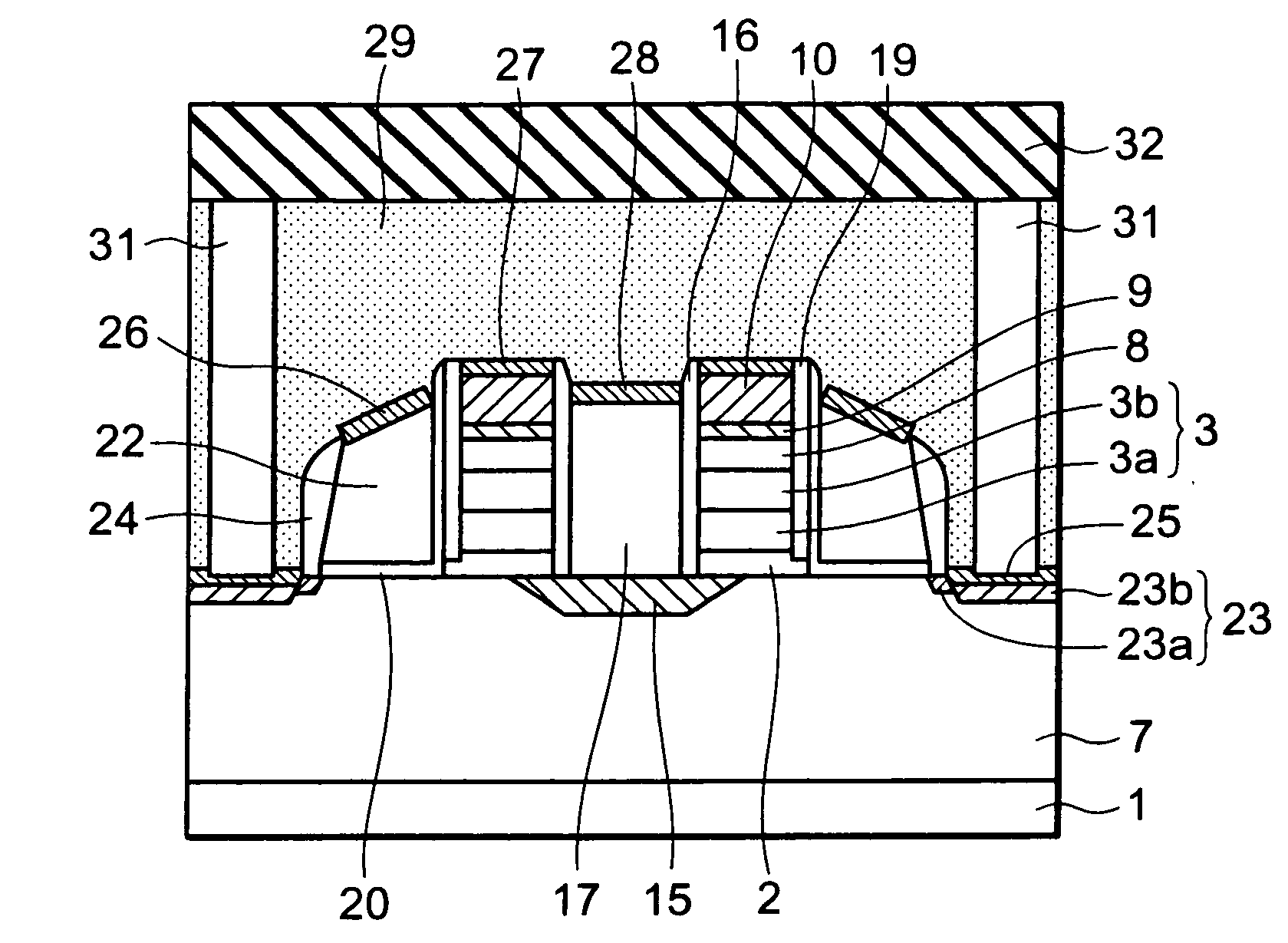
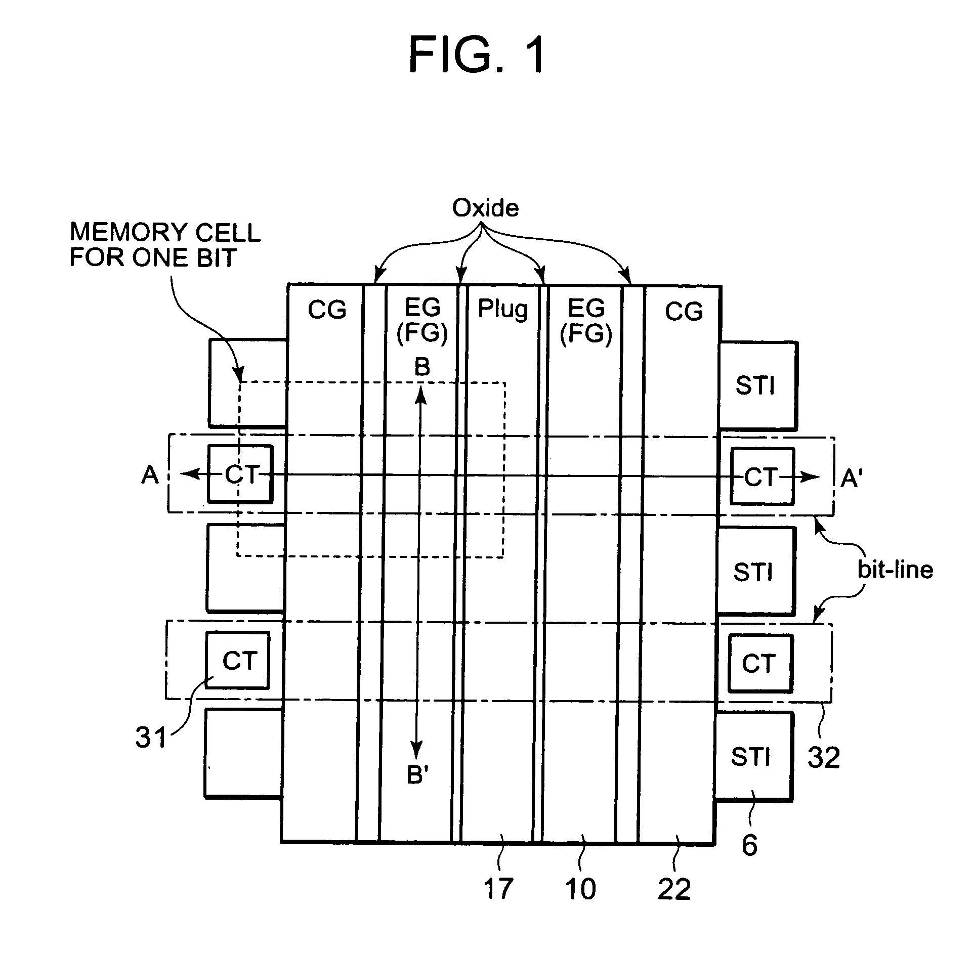
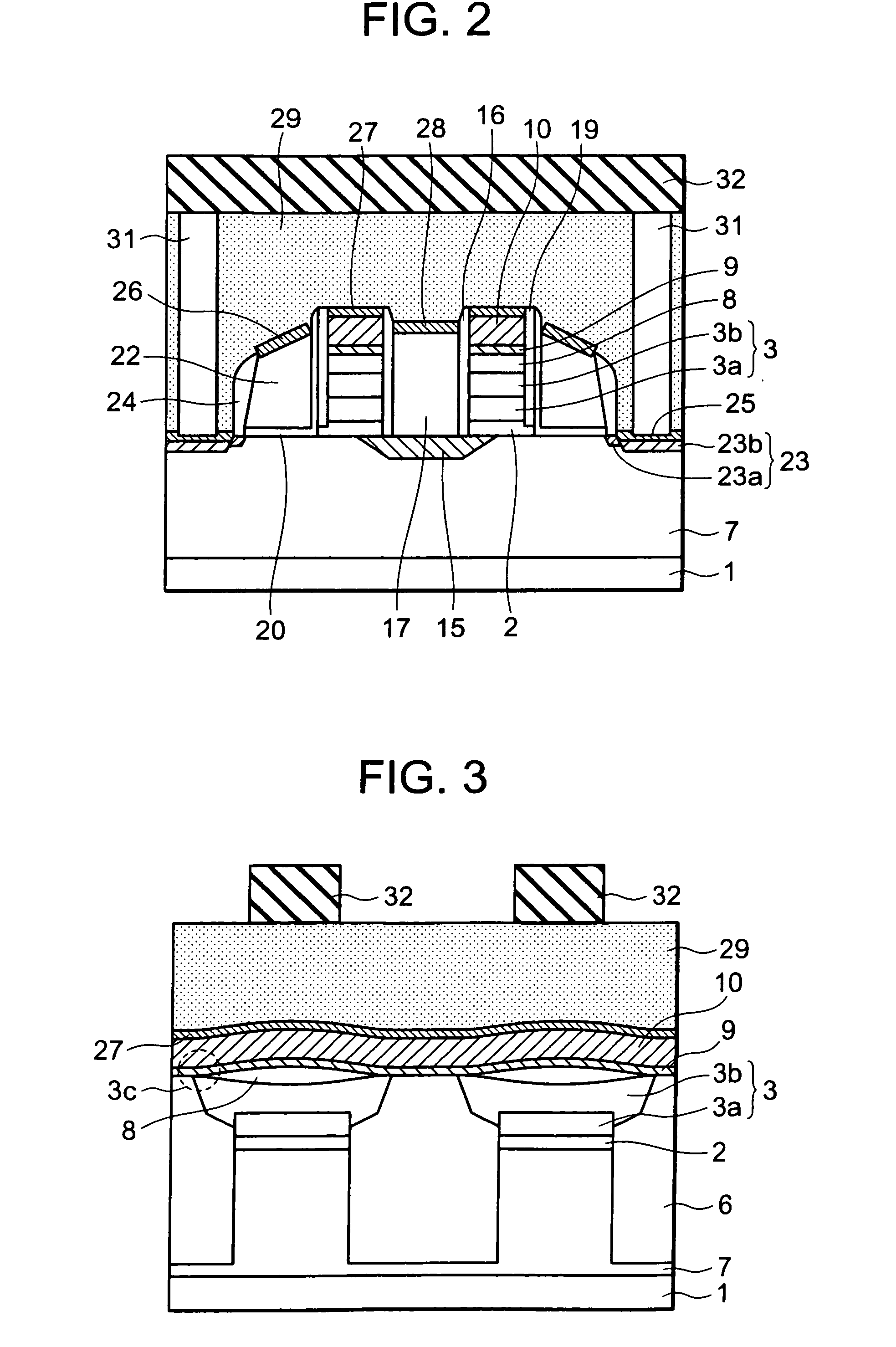
[0092]FIG. 1 to FIG. 3 are a plan view and cross sectional views of a non-volatile semiconductor memory device according to a first embodiment of the present invention. FIG. 1 illustrates a plan view (plane layout) viewed from upward. In FIG. 1, four pieces of the memory cells (four pieces of memory cells each being capable of recording data for one bit) are illustrated, and a portion surrounded by a dotted line in the figure corresponds to a memory cell for one bit.

[0093]AS illustrated in FIG. 1, a plug (PLUG) 17, an erasing gate (EG) 10, and a control gate (CG) 22, which are connected to a first source / drain diffusion layer 15, are formed in a direction parallel to a B-B′ direction. The erasing gate 10 and a control gate 22 are disposed in symmetric with respect to the plug 17. The plug 17, the erasing gate 10, and the control gate 22 are each electrically isolated by an insulating film (for example, oxide film). The plug 17, the erasing gate 10, and th...


PUM


Abstract

A non-volatile semiconductor memory device includes: a floating gate formed above the semiconductor substrate; an erasing gate formed above the floating gate; a control gate formed above a channel region of a surface layer of the semiconductor substrate at a position corresponding to one lateral side of the floating gate and the erasing gate; a diffusion layer formed on the semiconductor substrate at a position corresponding to another lateral side of the floating gate and the erasing gate; a plug formed above the diffusion layer, the plug coupled to the diffusion layer; a first silicide film formed on an upper surface of the erasing gate; and a second silicide film formed on an upper surface of the plug, in which a height of the upper surface of the plug is flush with/or lower than a height of the upper surface of the erasing gate.

Description

BACKGROUND OF THE INVENTION[0001]1. Field of the Invention[0002]The present invention relates to a non-volatile semiconductor memory device, and more particularly, to a non-volatile semiconductor memory device having an erasing gate.[0003]2. Description of the Related Art[0004]There is known a non-volatile semiconductor memory device having a floating gate as a non-volatile semiconductor memory device capable of retaining storage data even if a power source is turned off. In such a non-volatile semiconductor memory device described above, programming and erasing of the storage data may be performed through accumulation and release of an electric field with respect to the floating gate.[0005]Further, as one kind of the non-volatile semiconductor memory devices having a floating gate, various split-gate type non-volatile semiconductor memory devices are proposed. FIG. 46 illustrates an example of a prior art split-gate type non-volatile semiconductor memory device.[0006]As illustrated...

Claims


Application Information

Patent Timeline
IPC IPC(8): H01L47/00
CPCH01L21/28273H01L29/7881H01L29/42328H01L27/11521H01L29/40114H10B41/30
Inventor NAGAI, TAKAAKI
Owner RENESAS ELECTRONICS CORP
Why Eureka
Try Eureka