

Semiconductor integrated device
- Summary
- Abstract
- Description
- Claims
- Application Information
AI Technical Summary
Benefits of technology
Problems solved by technology
Method used
Image

Examples
first exemplary embodiment
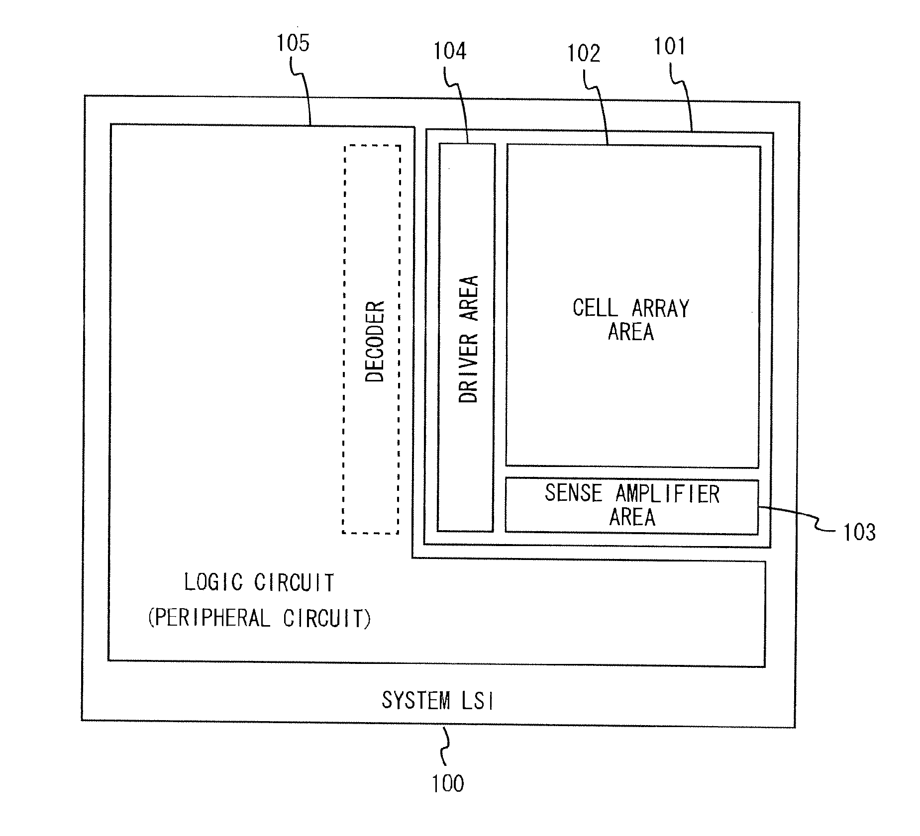
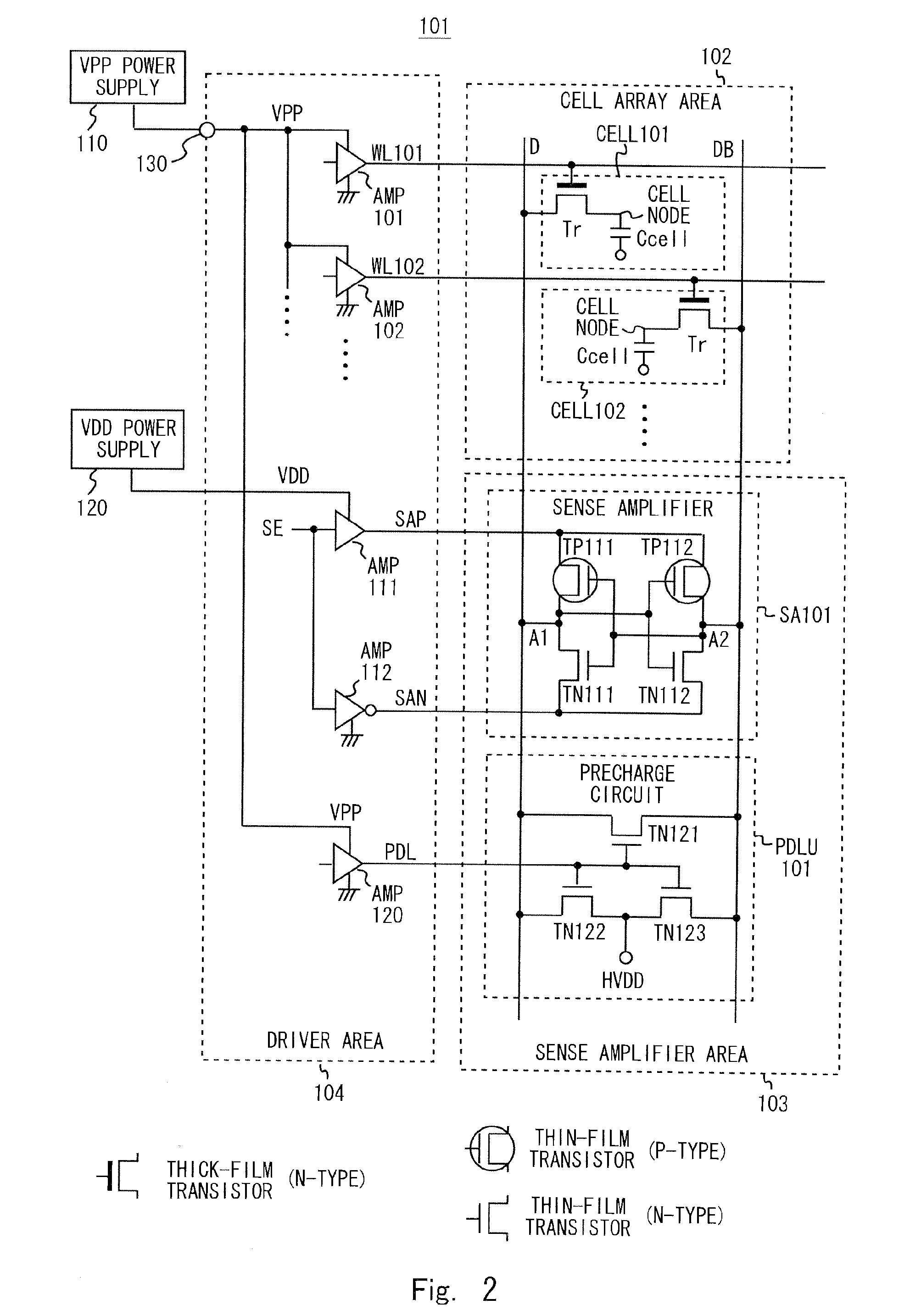
[0043]A first exemplary embodiment of the present invention will be described in detail below with reference to the accompanying drawings. In the first exemplary embodiment, the present invention is applied to a semiconductor integrated device 100 such as a system LSI. FIG. 1 shows a schematic diagram of a system LSI chip of the semiconductor integrated device 100. As shown in FIG. 1, the semiconductor integrated device 100 includes a semiconductor memory circuit 101 and a logic circuit 105.
[0044]The logic circuit 105 includes, integrated therein, a control circuit, such as a CPU of the semiconductor integrated device 100, and a logic gate for performing logic operation, such as an address decoder of the semiconductor memory circuit 101. The semiconductor integrated device 100, such as a system LSI, is required to have a high performance. For this reason, the logic gate constituting the logic circuit 105 is required to execute a logic operation at high speed. Therefore, in the logic...
second exemplary embodiment
[0077]A second exemplary embodiment of the present invention will be described in detail with reference to the drawings. In the second exemplary embodiment, the present invention is applied to a semiconductor integrated device such as a system LSI, as with the first exemplary embodiment. A semiconductor integrated device 200 according to the second exemplary embodiment differs from the semiconductor integrated device of the first exemplary embodiment in the configuration of a semiconductor memory circuit portion. Assuming that a semiconductor memory circuit according to the second exemplary embodiment is a semiconductor memory circuit 201, the semiconductor integrated device 200 of the second exemplary embodiment has a configuration in which the semiconductor memory circuit 101 of the semiconductor integrated device 100 shown in FIG. 1 is replaced with the semiconductor memory circuit 201.
[0078]The semiconductor integrated device 200 includes the semiconductor memory circuit 201 and...
PUM
 Abstract
Description
Claims
Application Information