

Semiconductor memory device
- Summary
- Abstract
- Description
- Claims
- Application Information
AI Technical Summary
Benefits of technology
Problems solved by technology
Method used
Image

Examples
embodiment 1
Typical embodiments of the second aspect of the invention will be described referring to the accompanying drawings.
In the drawings, the same reference numeral designates the same or like parts.
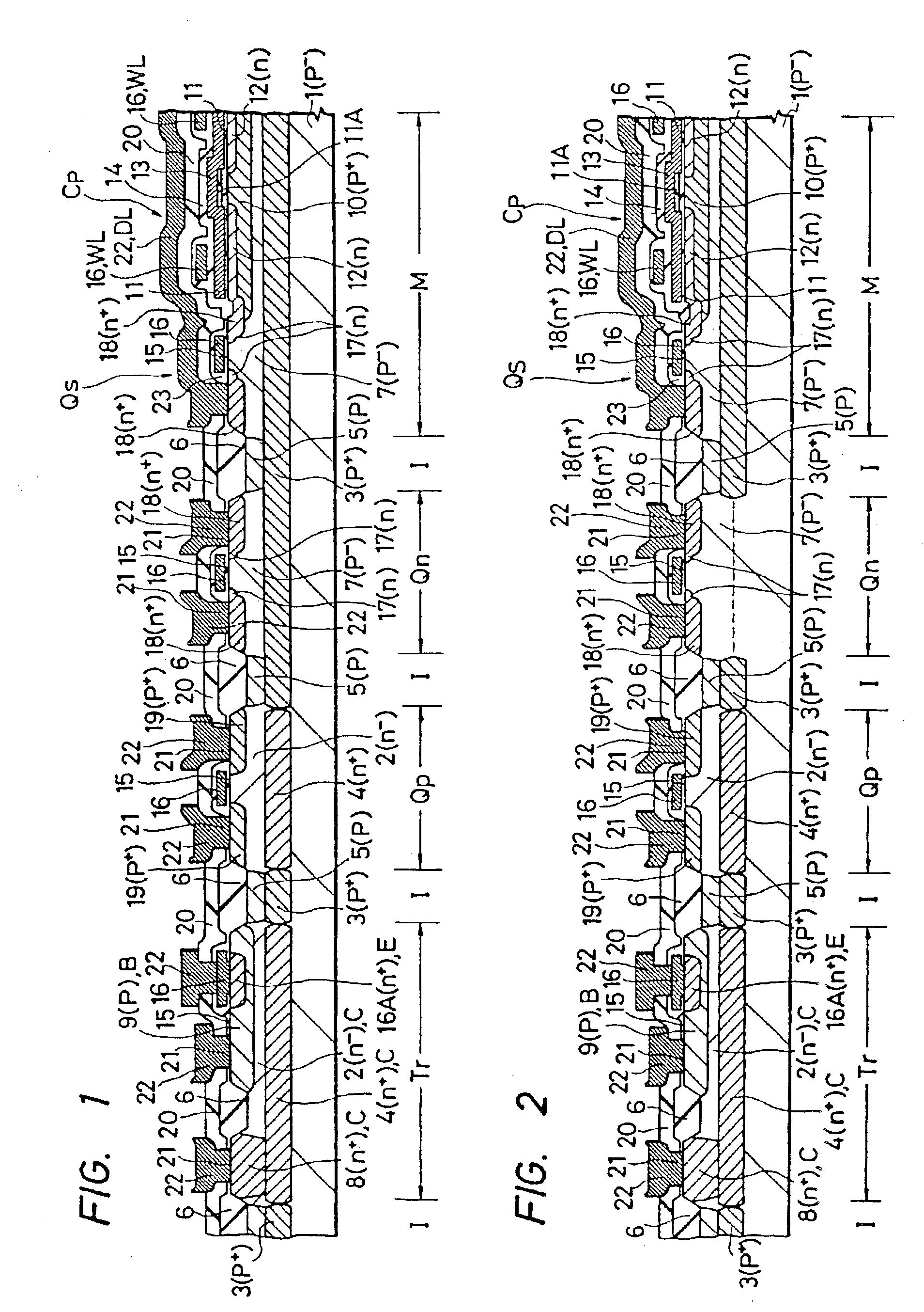
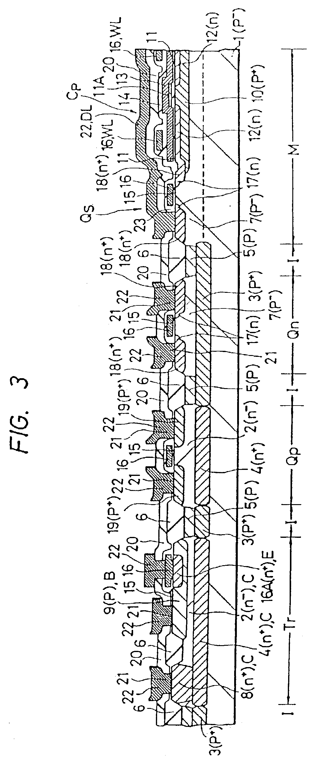
FIG. 19, FIG. 20, FIG. 21 and FIG. 22 show an embodiment of a semiconductor memory according to this aspect of the invention.
The semiconductor memory shown in FIG. 19-FIG. 22 is a static RAM using a Bi-CMOS type logical circuit in the peripheral circuit, and the basic constitution is similar to that shown in FIG. 14-FIG. 16.
FIG. 22 shows the outline of whole constitution of the static RAM 1100.
As shown in FIG. 22, the static RAM 1100 is formed on a single semiconductor substrate 1200. Most of the area of the substrate 1200 is occupied by a memory cell array unit 1120. The memory cell array unit 1120 is divided into a plurality of surfaces, and a peripheral circuit unit 1110 is arranged around each divided surface of the memory cell array unit 1120 and therebetween. Further, a terminal pad PAD ...
embodiment 2
A second embodiment of this second aspect of the invention will now be described referring to FIG. 24.
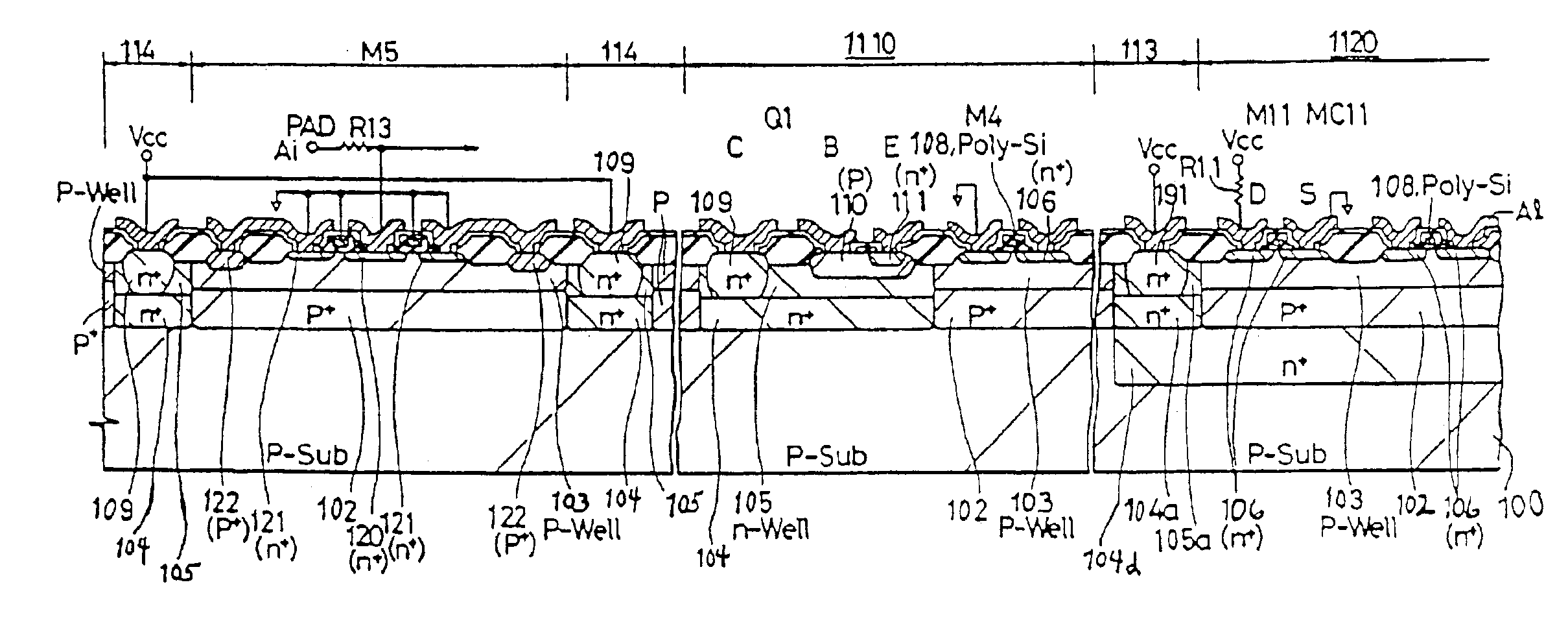
FIG. 24 is a device sectional view of the input protective element M5 disposed near the input pad, the peripheral circuit unit 1110 including the Bi-CMOS composite switching circuit; and the memory array 1120 including the memory cell. FIG. 24 illustrates prevention of information destruction in the memory cell when a signal of negative potential is applied to the input pad PAD. FIG. 24 shows structure where the input protective element M5 shown in FIG. 18 is added to the left of FIG. 21.
A feature of the second embodiment is in that the first minority carrier absorbing area 113 and the second minority carrier absorbing area 114 are formed. As a result, a signal of negative potential is inputted to the input pad PAD, and the potential of the drain n+ type layer 120 of the input protective element M5 becomes lower than the potential of the p type area 100, 102, 103. Even if the drain ...
embodiment 3
FIG. 25 is a device sectional view illustrating a third embodiment of this second aspect of the invention, and shows corresponding parts to the device sectional view shown in FIG. 24.
A difference of FIG. 25 from FIG. 24 is in that the n type buried layer 104b as a second buried layer is formed under the p type well layer 102 with the input protective element M5 formed thereon, and contacted with the second minority carrier absorbing area 114. Since the second minority carrier absorbing area (guard ring) is formed in ring shape so as to surround the input protective element M5, the p type well layer 103 with the input protective element M5 formed thereon is independent electrically of the p type substrate 100. Consequently, even if the drain 120 of the input protective element M5 acquires a negative potential due to the static electricity, ions injected from the drain into the p type well layer 103 can be securely absorbed in the n+ type buried layer 102a with Vcc potential and the s...
PUM
 Abstract
Description
Claims
Application Information