Semiconductor storage device and method of manufacturing same

A technology of a storage device and a manufacturing method, which is applied in semiconductor/solid-state device manufacturing, semiconductor devices, semiconductor/solid-state device components, etc., can solve problems such as reliability readout interference reduction, and improve design freedom and reliability Effect

Inactive Publication Date: 2007-09-19
NEC ELECTRONICS CORP
View PDF2 Cites 4 Cited by
  • Summary
  • Abstract
  • Description
  • Claims
  • Application Information

AI Technical Summary

Problems solved by technology

Therefore, there is a risk that operational reliability (in particular, read disturbance characteristics) will be reduced.

Method used


Image

  • Semiconductor storage device and method of manufacturing same
  • Semiconductor storage device and method of manufacturing same
  • Semiconductor storage device and method of manufacturing same

Examples


Embodiment approach 1

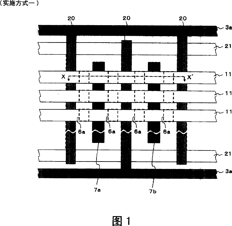
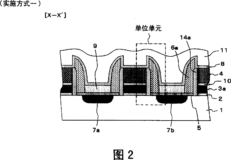
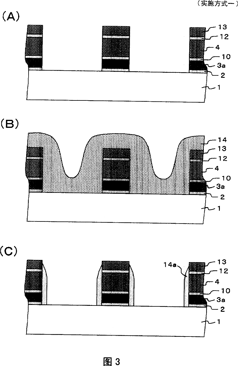
[0057] A semiconductor memory device according to Embodiment 1 of the present invention will be described with reference to the drawings. FIG. 1 is a partial plan view schematically showing the configuration of a semiconductor memory device according to Embodiment 1 of the present invention. 2 is a partial cross-sectional view along line X-X' (in FIG. 1 ) schematically showing the configuration of the semiconductor memory device according to Embodiment 1 of the present invention.

[0058] The semiconductor memory device according to Embodiment 1 is a nonvolatile semiconductor memory device that stores two bits of information in one cell. The semiconductor storage device has: a substrate 1, an insulating film 2, a selection gate 3a, an insulating film 10, an insulating film 4, an insulating film 5, side walls 14a, a floating gate 6a, a first diffusion region 7a, a second diffusion region 7b, an insulating film 8, insulating film 9, control gate 11, and third diffusion region 2...


PUM


Abstract

The semiconductor memory device comprises: a select gate 3a formed in a first region on a substrate 1; the floating gate 6a formed in a second region adjacent to the first one; a second diffusion region 7b formed in a third region adjacent to the second one; and the control gate 11 formed on the floating gate. The coupling capacitance between the select gate 3a and the floating gate 6a is set smaller than that between the substrate 1 and the floating gate 6a. The thickness of a side wall 14a between the select gate 3a and the floating gate 6a is larger than that of an insulation film 5 between the substrate 1 and the floating gate 6a.To increase the ratio of the coupling capacitance between a floating gate and a control gate to the total capacitance, and to improve the reliability during the read-out operation.

Description

technical field [0001] The present invention relates to a semiconductor storage device with cell transistors and a manufacturing method thereof, in particular to a semiconductor storage device storing multi-bit information in one cell and a manufacturing method thereof. Background technique [0002] Among conventional semiconductor memory devices, a nonvolatile semiconductor memory device (conventional example 1) shown in FIGS. 9 and 10 is known as a nonvolatile semiconductor memory device that stores multi-bit information in one cell. In the nonvolatile semiconductor memory device according to Conventional Example 1, the memory cell is provided with: a first diffusion region 107a and a second diffusion region 107b separately provided in parallel on the surface of the substrate 101; The selection gate 103a on the substrate 101 in the region between the first diffusion region 107a and the second diffusion region 107b; and the third diffusion region (121 in FIG. The substrate...

Claims


Application Information

Patent Timeline
Patent Type & Authority Applications(China)
IPC IPC(8): H01L27/115H01L23/522H01L21/8247H01L21/768
CPCH01L27/11521H01L29/7883H01L29/42324H01L27/115H10B69/00H10B41/30
Inventor 池田雄次
Owner NEC ELECTRONICS CORP
Why Eureka
Try Eureka