Illuminator packaging structural capable of preventing electrostatic damaged and manufacturing method therefor

A technology of packaging structure and electrostatic destruction, applied in the direction of electric solid devices, circuits, electrical components, etc., can solve the problems of low thermal resistance of metal materials, hindering the output beam, thickness limitation, etc., and achieve the effect of low thermal resistance and excellent heat dissipation

Inactive Publication Date: 2007-09-26
IND TECH RES INST
View PDF2 Cites 5 Cited by
  • Summary
  • Abstract
  • Description
  • Claims
  • Application Information

AI Technical Summary

Problems solved by technology

[0010] 3. The solder balls 307 and 308 should not be too large, otherwise it will easily cause a short circuit between the P pole 321 and the N pole 320 of the Zener diode 302;
[0011] 4. Using a silicon diode whose thickness cannot be reduced as a carrier substrate, the heat dissipation effect is not ideal, and it is still not as low as the thermal resistance of a metal material
[0014] 1. If the light-emitting diode is electrically connected to the outside by front-side bonding, the heat dissipation path must pass through the thermally conductive low-fat sapphire substrate, and the thermal resistance cannot be reduced
[0015] 2. If the wires and line pads are located in the light emitting directio

Method used


Image

  • Illuminator packaging structural capable of preventing electrostatic damaged and manufacturing method therefor
  • Illuminator packaging structural capable of preventing electrostatic damaged and manufacturing method therefor
  • Illuminator packaging structural capable of preventing electrostatic damaged and manufacturing method therefor

Examples


Embodiment Construction

[0078] The technical means and functions used to achieve the purpose of the present invention will be described below with reference to the accompanying drawings, and the embodiments listed below with the accompanying drawings are only for auxiliary illustration, and the technical means of this case are not limited thereto.

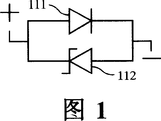
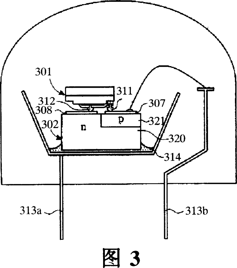
[0079] First please refer to a preferred embodiment of the present invention shown in FIG. 6, the light emitter packaging structure 10 that can prevent electrostatic damage, which is mainly composed of a light emitting diode 2, two carrying bases 3, 4, and an electrostatic protection component 5. .

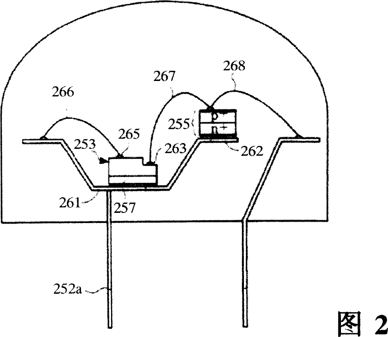
[0080] The light-emitting diode 2 is a chip-type light-emitting diode with a P-type electrode 21 and an N-type electrode 22 , and is disposed on the two carrying bases 3 , 4 . It must be noted that the light emitting diode 2 can be any other solid-state light source capable of emitting light energy, and is not limited to light emitting diodes.

[0081] The t...


PUM

PropertyMeasurementUnit
Thicknessaaaaaaaaaa
Thermal expansion coefficientaaaaaaaaaa
Thicknessaaaaaaaaaa

Abstract

The invention relates to illuminator encapsulation structure which can avoid the destroy of static and manufacturing method, it at least includes a illuminator which is set on at least two metal material loading bases which possess high conductive and high heat-conducting coefficient, the two loading bases are separately connected with the positive and negative pole, wafer type static protecting subassembly is glued between the two loading bases, so the illuminator can possesses best radiating path under high power, and the damage caused by static projecting wave to illuminator can be prevented.

Description

technical field [0001] The present invention relates to a light emitting device packaging structure that can prevent electrostatic damage, in particular to a packaging technology applied to high-power light-emitting diode point light sources or high-power light-emitting diode light source modules. The antistatic components contained in it can be respectively Applied to a single package structure, polycrystalline series structure or polycrystalline parallel structure, in addition to having the function of electrostatic protection, it also has a low thermal resistance value and excellent heat dissipation capability. Background technique [0002] Since the 1960s, light-emitting diodes (LEDs, Light Emitting Diodes) made of gallium arsenide (GaAs) and aluminum gallium indium phosphide (AlGaInP) have obtained red to yellow-green wavelengths in the form of electroluminescence. In recent years, due to the breakthrough of gallium nitride (GaN) materials in epitaxy technology, blue an...

Claims


Application Information

Patent Timeline
IPC IPC(8): H01L33/00H01L23/60H01L25/16H01L33/48H01L33/64
CPCH01L2224/32245H01L2224/48091H01L2924/0002H01L2224/73265H01L2224/48247H01L2224/48137H01L2924/12032H01L2924/00014H01L2924/00
Inventor 周明杰林文山蔡宏欣
Owner IND TECH RES INST
Why Eureka
Try Eureka