Single programmable memory and its making method

A manufacturing method and memory technology, which are used in semiconductor/solid-state device manufacturing, electric solid-state devices, semiconductor devices, etc., can solve the problems of reducing memory operation efficiency and small channel current, and achieve the effect of increasing the width and improving the channel current.

Inactive Publication Date: 2007-10-31
POWERCHIP SEMICON CORP
View PDF1 Cites 2 Cited by
  • Summary
  • Abstract
  • Description
  • Claims
  • Application Information

AI Technical Summary

Problems solved by technology

However, since silicon nitride has the characteristic of trapping charges, part of the charges stored in the floating gate will f

Method used


Image

  • Single programmable memory and its making method
  • Single programmable memory and its making method
  • Single programmable memory and its making method

Examples


Embodiment Construction

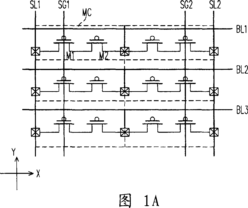
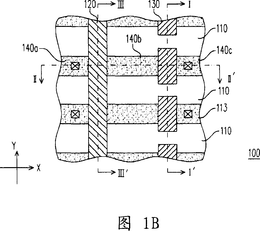
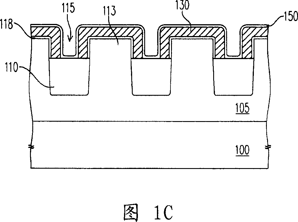
[0054] FIG. 1A is a schematic circuit diagram of a one-time programmable memory according to an embodiment of the present invention. FIG. 1B is a top view illustrating a one-time programmable memory according to an embodiment of the present invention. Fig. 1C is a schematic cross-sectional view along line I-I' of Fig. 1B. Fig. 1D is a schematic cross-sectional view along line II-II' of Fig. 1B. Fig. 1E is a schematic cross-sectional view along line III-III' of Fig. B.

[0055]Please refer to FIG. 1A , FIG. 1B , FIG. 1C , FIG. 1D and FIG. 1E . The one-time programmable memory proposed by the present invention is, for example, composed of a substrate 100, a plurality of isolation structures 110, a plurality of memory cells MC, selection gate lines SG1, SG2, source lines SL1, SL2, and bit lines BL1, BL2, BL3. consist of.

[0056] The substrate 100 is, for example, a silicon substrate. The isolation structure 110 is, for example, disposed in parallel in the substrate 100 and ...


PUM


Abstract

The invention discloses a single-time programmable memory that comprises basis, several separation configurations, the first transistor and the second transistor. The separation configurations are set on the basis to define the active area. Each of the separation configurations possesses depression to make the top surface of the separation configuration lower than the basis. The first transistor is set on the active area of the basis, and extends to the sidewall of the depression, the gate electrode of the first transistor is selecting gate electrode. The second transistor is set on the active area of the basis, serially connected with the first transistor. The gate electrode of the second transistor is float gate electrode which is block type and bestrides over the basis of the separation configurations, and extends to the sidewall of the depression.

Description

technical field [0001] The present invention relates to a non-volatile memory and its manufacturing method, and in particular to a one-time programmable memory and its manufacturing method. Background technique [0002] Non-volatile memory can be subdivided into mask mode read-only memory (Mask ROM), erasable and programmable read-only memory (Erasable Programmable ROM; EPROM), electrically erasable and programmable Read Only Memory (Electrically Erasable Programmable ROM; E 2 PROM), one-time programmable read-only memory (One Time Programmable ROM; OTPROM), etc. [0003] US Patent No. 6,678,190 discloses a one-time programmable read-only memory, using two series-connected P-type transistors disposed on an N-well as a selection gate and a floating gate, respectively. Since there is no need to configure a control gate, it has the advantage of being able to be integrated with a CMOS process. [0004] However, with the development of the integrated circuit industry, the goal...

Claims


Application Information

Patent Timeline
IPC IPC(8): H01L27/115H01L21/8247
Inventor 张格荥黄宗正黄彦宏
Owner POWERCHIP SEMICON CORP
Why Eureka
Try Eureka