Method for making solder bump

A technology of solder bumps and fabrication methods, applied in the fields of semiconductor/solid-state device manufacturing, electrical components, electrical solid-state devices, etc., can solve problems such as the influence of solder bumps and the reliability of semiconductor devices

Inactive Publication Date: 2007-11-14
SEMICON MFG INT (SHANGHAI) CORP
View PDF0 Cites 8 Cited by
  • Summary
  • Abstract
  • Description
  • Claims
  • Application Information

AI Technical Summary

Problems solved by technology

Negatively impacts the reliability of solder bumps and semiconductor devices

Method used


Image

  • Method for making solder bump
  • Method for making solder bump
  • Method for making solder bump

Examples


Embodiment Construction

[0061] Below by embodiment, the present invention is described in more detail.

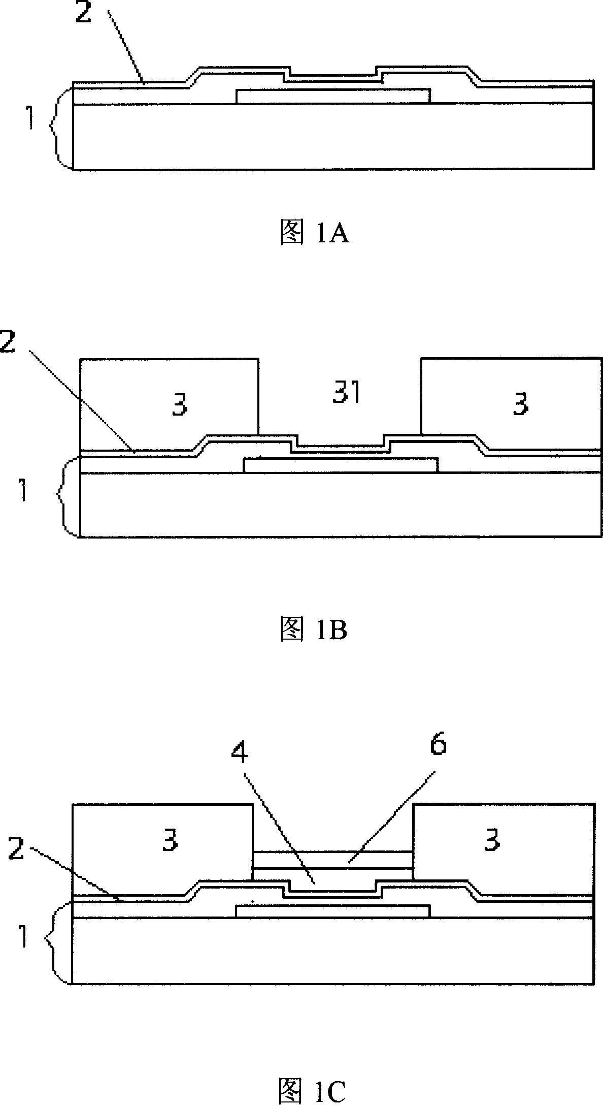
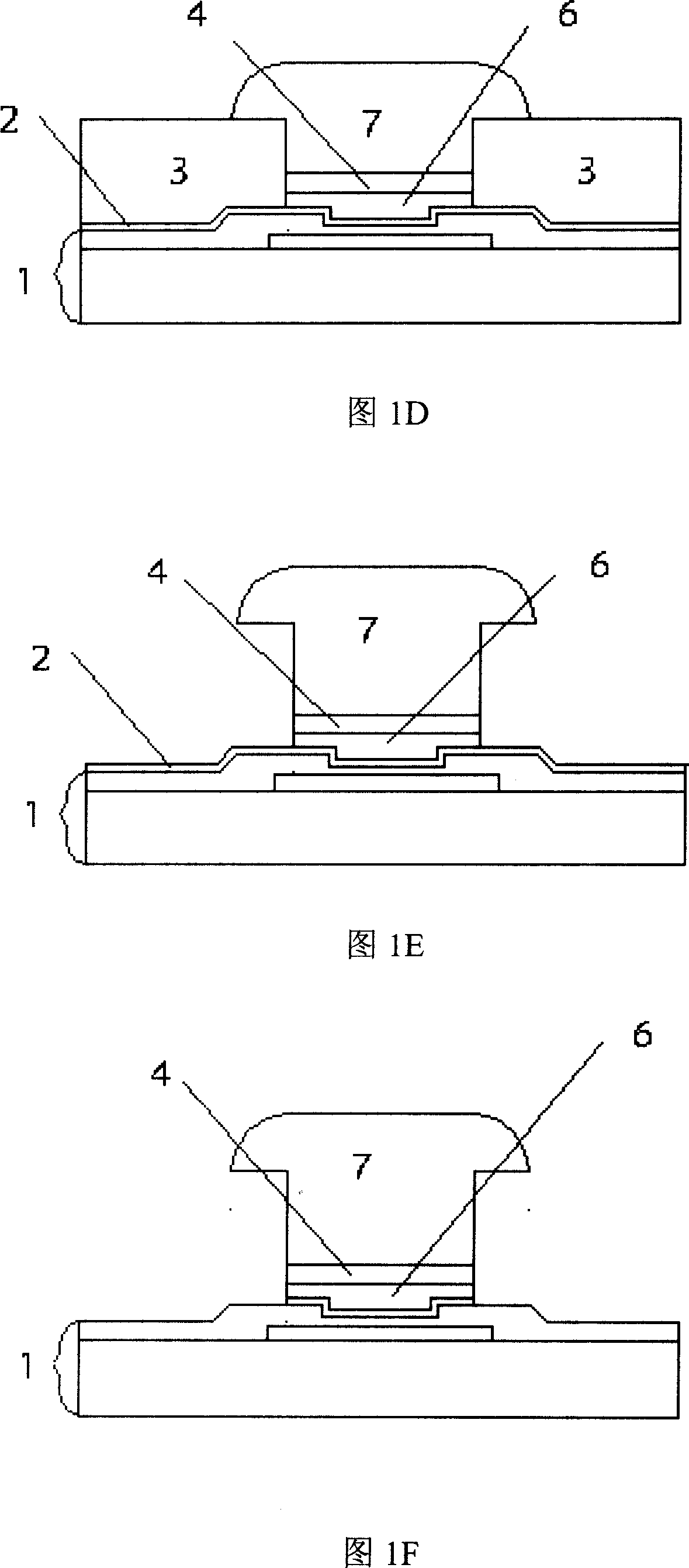
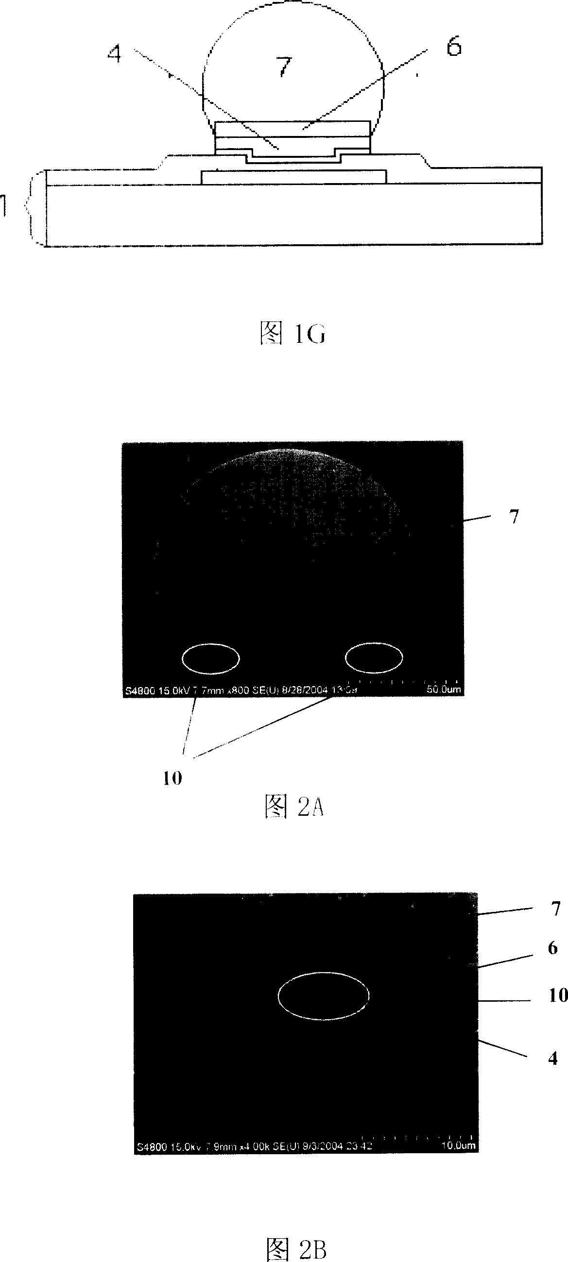
[0062] In the wafer level redistribution package (Wafer Level Contribution Package, WLCSP), first make the pads on the IC wafer and cover the passivation layer around the pads, generally as a prefabricated layer 21, as shown in FIG. 3A. A chrome-copper (Cr-Cu) layer 22 is then sputter deposited using conventional techniques around the pad area where the solder bump is to be formed. Wherein, first sputtering deposits a chromium (Cr) layer, the thickness of the chromium (Cr) layer is 1000±50 Ȧ; then sputtering deposits a copper (Cu) layer, the thickness of the copper (Cu) layer is 3000±100 Ȧ, The total thickness of the chromium-copper (Cr—Cu) layer 22 is 4000±150 Ȧ.

[0063] As shown in Figure 3B, the first photoresist (PR) layer 23 is coated on the above-mentioned chromium-copper (Cr-Cu) layer 22, and the thickness of the photoresist layer is 7 ± 0.5 μm, and photolithography is carried out accordi...


PUM

PropertyMeasurementUnit
thicknessaaaaaaaaaa
thicknessaaaaaaaaaa
thicknessaaaaaaaaaa

Abstract

The invention provides a new solder bump making method, able to prevent metal layers under solder bumps from being over etched. And it is characterized in: separately forming plated copper layers under solder bumps and nickel isolation layers on the plated copper layers and making the nickel isolation layers completely cover the plated copper layers under them to prevent the plated copper layers from being etched in the following isotropic etching and forming bottom cut, i.e. concave cut, in all plated copper layers. Thus, it can prevent the conductivity of the formed solder bumps from decreasing and improves reliability of solder bumps and semiconductor devices.

Description

technical field [0001] The present invention relates generally to methods of making solder bumps, and more particularly to methods of making solder bumps that prevent over-etching of the metal layer beneath the solder bumps. Background technique [0002] A large number of solder bumps for connection need to be formed in semiconductor devices. Under the solder bumps, a metal layer must be formed to connect with the various conductive connection lines in the semiconductor device. Usually, the metal layer under the solder bumps includes a copper metal layer, and the solder bumps are electroplated lead (Pb)-free tin-silver ( Sn-Ag) metal composition. The copper under the solder bumps is easy to diffuse into the solder bumps to form a Sn-Ag-Cu eutectic, which reduces the conductivity of the solder bumps. In order to prevent copper from diffusing into the solder bumps, a nickel (Ni) metal layer is formed on top of the copper metal layer as an isolation layer. The copper metal l...

Claims


Application Information

Patent Timeline
Patent Type & Authority Applications(China)
IPC IPC(8): H01L21/60
CPCH01L24/11H01L2224/11H01L2924/00012
Inventor 钟志明李德君
Owner SEMICON MFG INT (SHANGHAI) CORP
Why Eureka
Try Eureka