
Semiconductor device and a method of manufacturing the same

A technology for semiconductors and devices, applied in the field of semiconductor devices and their manufacturing, can solve problems such as junction leakage, difficulty in fully ensuring the width of sidewall spacers, etc., and achieve the effect of preventing problems

Inactive Publication Date: 2007-11-14
RENESAS TECH CORP
View PDF3 Cites 10 Cited by
  • Summary
  • Abstract
  • Description
  • Claims
  • Application Information

AI Technical Summary

Problems solved by technology

Thereby, the size (width) of the underside of the sidewall spacer 12 along the gate length direction of the substrate 1 has been limited by the height of the separated grid, that is, the thickness of the control grid 8, so when the control grid 8 When the film thickness is made thin, it may be difficult to secure a sufficient width of the sidewall spacer 12
Thus, it is noted that in the n + The problem of junction leakage between the p-type semiconductor regions 10d, 10s and the p-type well 2 forming the junction surface

Method used


Image

  • Semiconductor device and a method of manufacturing the same
  • Semiconductor device and a method of manufacturing the same
  • Semiconductor device and a method of manufacturing the same

Examples


Embodiment Construction

[0050] Hereinafter, embodiments of the present invention will be explained with reference to the drawings. In all the drawings for explaining the embodiments, in principle the same reference numerals and symbols are used for the same elements, and repeated descriptions thereof are omitted.

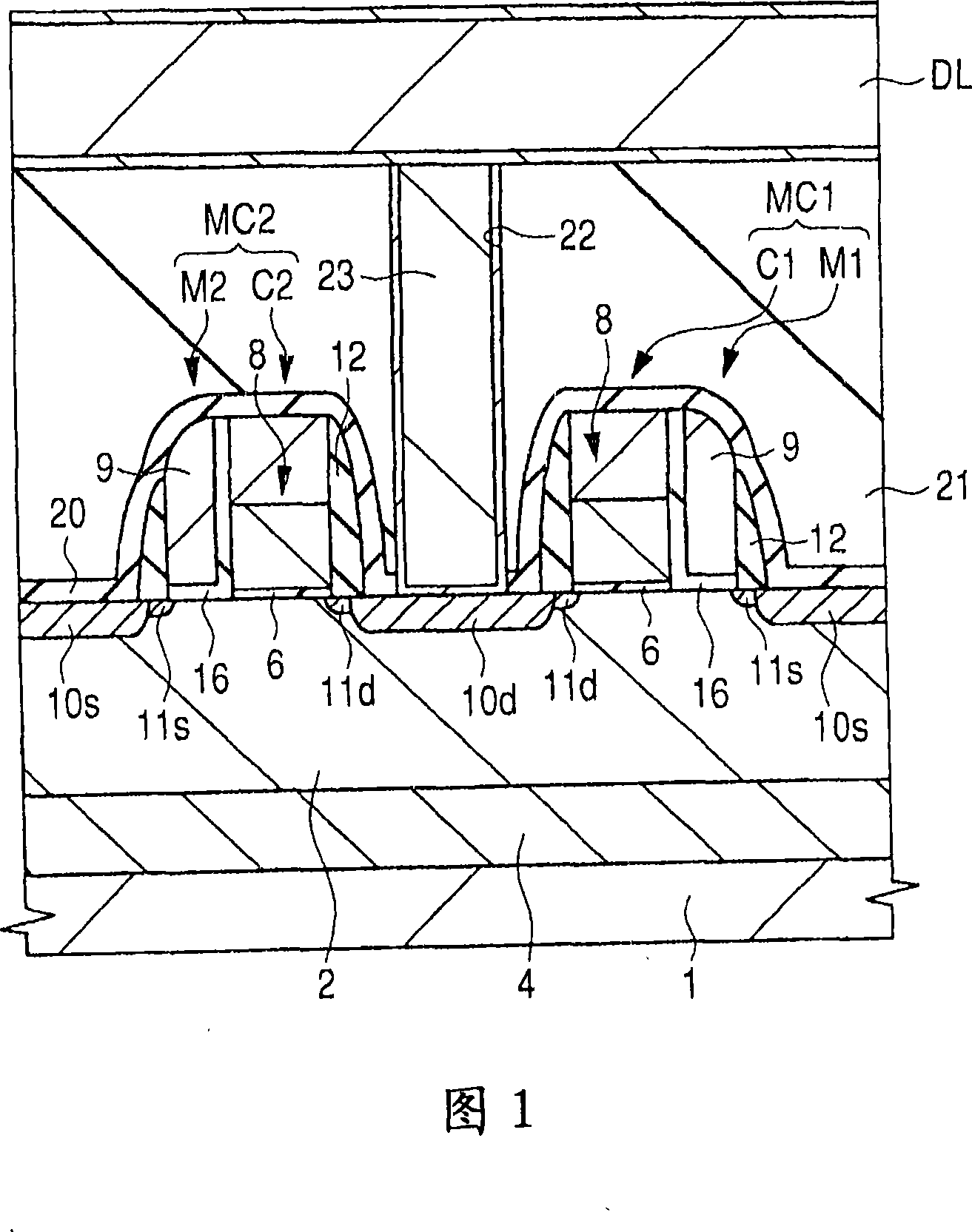
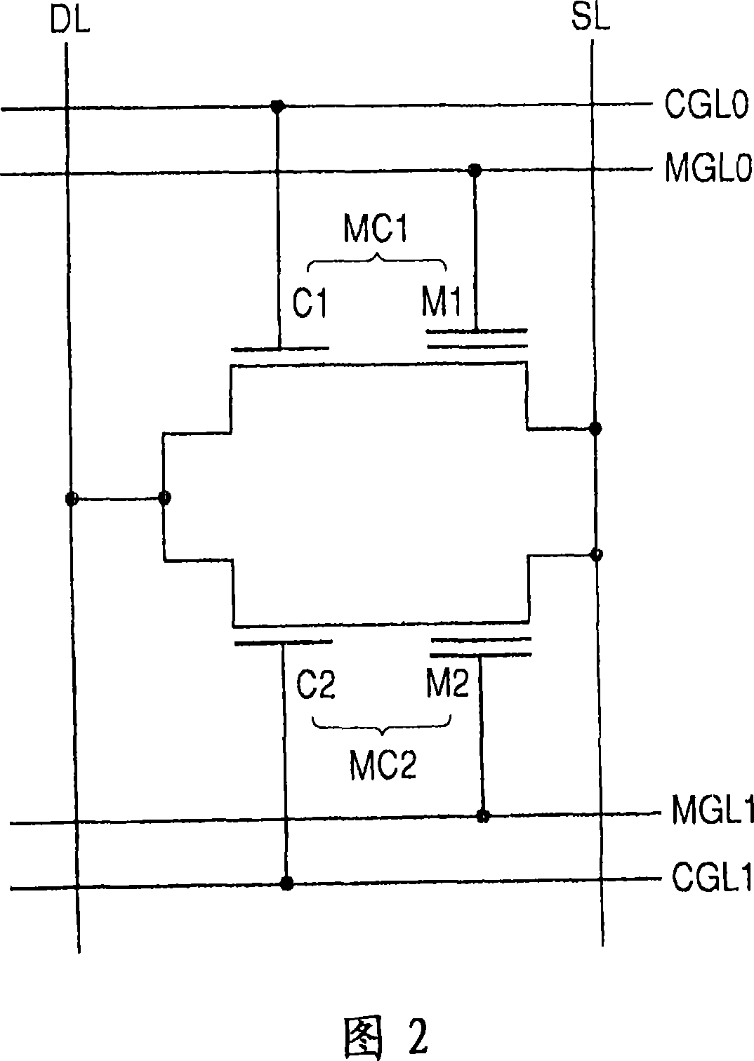
[0051] 1 is a cross-sectional view showing a relevant portion of a MONOS (Metal Oxide Nitride Oxide Semiconductor) type nonvolatile memory according to an embodiment, and FIG. 2 is a diagram of the MONOS type nonvolatile memory shown in FIG. 1. Equivalent circuit diagram. 1 and 2 show two memory cells (MC1, MC2) arranged adjacent to each other.

[0052] Memory cell MC1 as a MONOS type nonvolatile memory is formed at p-type well 2 in semiconductor substrate 1 (hereinafter, simply referred to as "substrate") made of a p-type single crystal silicon substrate or the like. The p-type well 2 to which a desired voltage is applied is electrically separated from the substrate 1 by an n-type embed...


PUM


Abstract

In a semiconductor device which includes a split-gate type memory cell having a control gate and a memory gate, a low withstand voltage MISFET and a high withstand voltage MISFET, variations of the threshold voltage of the memory cell are suppressed. A gate insulating film of a control gate is thinner than a gate insulating film of a high withstand voltage MISFET, the control gate is thicker than a gate electrode 14 of the low withstand voltage MISFET and the ratio of thickness of a memory gate with respect to the gate length of the memory gate is larger than 1. The control gate and a gate electrode 15 are formed in a multilayer structure including an electrode material film 8 A and an electrode material layer 8 B, and the gate electrode 14 is a single layer structure formed at the same time as the electrode material film 8 A of the control gate.

Description

[0001] Cross References to Related Applications [0002] The disclosure of Japanese Patent Application No. 2006-131208 filed on May 10, 2006 including specification, drawings and abstract is incorporated herein by reference in its entirety. technical field [0003] The present invention relates to a semiconductor device and its manufacturing method, and more particularly, to a technique effective when applied to the manufacture of a semiconductor device including a nonvolatile memory and its peripheral circuits. Background technique [0004] As a nonvolatile memory (electrically erasable and programmable read-only memory) in which data can be rewritten electrically, a split gate type using a charge storage layer including an ONO (Oxide Nitride Oxide) film is known storage unit structure. [0005] As a peripheral circuit of a nonvolatile memory, for example, a circuit including a low withstand voltage MISFET such as a sense amplifier, a column decoder, and a row decoder, an...

Claims


Application Information

Patent Timeline
IPC IPC(8): H01L27/115H01L29/423H01L21/8247H01L21/336H01L21/28
CPCH01L21/823462H01L27/0629H01L27/11526H01L27/115H01L27/11546H01L27/0922H01L29/6653H01L27/105H01L27/11568H10B41/40H10B41/49H10B43/30H10B69/00
Inventor 石井泰之桥本孝司川岛祥之鸟羽功一町田悟片山弘造齐藤健太郎松井俊一
Owner RENESAS TECH CORP
Features
  • Generate Ideas
  • Intellectual Property
  • Life Sciences
  • Materials
  • Tech Scout
  • Unparalleled Data Quality
  • Higher Quality Content
  • 60% Fewer Hallucinations
Learn More