Light emitting device and method of manufacturing the same

A technology for a light-emitting device and a manufacturing method, which is applied to the manufacturing of semiconductor/solid-state devices, electrical components, and electrical solid-state devices, etc., can solve problems such as difficulty in long-term use, complicated manufacturing processes, and difficult light reflection, and achieve simple manufacturing processes. simplification, process simplification, and good reflection efficiency

Inactive Publication Date: 2007-11-28
ELEMENT DENSHI
View PDF1 Cites 3 Cited by
  • Summary
  • Abstract
  • Description
  • Claims
  • Application Information

AI Technical Summary

Problems solved by technology

[0006] A hole is formed in the base substrate corresponding to the back surface on which the light-emitting element is mounted, and the light emitted from the bottom of the light-emitting element is reflected upward, so the heat dissipation is not good, and there is a problem that it is difficult to use for a long time
[0007] In addition, since the hole is formed by cutting in the thickness direction of the base substrate, the hole is covered by the light emitting element, and it is difficult to increase the amount of light reflection.
[0008] In addition, in order to improve the brightness of the light-emitting element, it is necessary to perform etching on the base substrate to form a concave portion, and to form a light-reflecting portion on the surface opposite to the surface on which the light-emitting element is placed or the inner peripheral surface of the hole. There is also a problem that the manufacturing process is complicated

Method used


Image

  • Light emitting device and method of manufacturing the same
  • Light emitting device and method of manufacturing the same
  • Light emitting device and method of manufacturing the same

Examples


Embodiment Construction

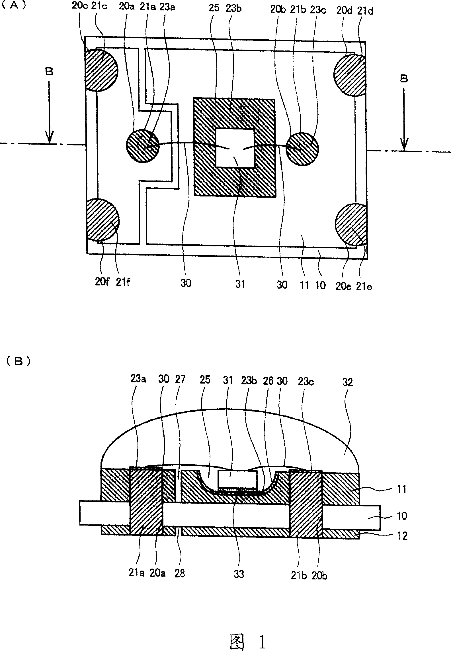
[0048] First, FIG. 1 shows a light emitting device of the present invention. FIG. 1(A) is a top view thereof, and FIG. 1(B) is a cross-sectional view thereof.

[0049] The light-emitting device of the present invention includes: an insulating substrate 10, a thick first conductive foil 11 arranged on one main surface of the insulating substrate 10, a thin second conductive foil 12 arranged on the opposite main surface of the insulating substrate 10, and a thin second conductive foil 12 arranged on the second main surface of the insulating substrate 10. A half-etched hole 25 on a conductive foil 11, a light emitting element 31, through-hole electrodes 21a, 21b, 21c, 21d, 21e, 21f connecting the first conductive foil 11 and the second conductive foil 12, conductive metal layers 23a, 23b , 23c, thin metal wire 30 and transparent protective resin 32.

[0050] It is preferable to use a glass epoxy substrate or a glass polyimide substrate as the insulating substrate 10 . It functi...


PUM

PropertyMeasurementUnit
thicknessaaaaaaaaaa
thicknessaaaaaaaaaa

Abstract

A light emitting device of the present invention includes a first conductive film, a second conductive film, a half-etching hole, a light emitting element, through-hole electrodes, conductive metal layers, metallic wires and a transparent protective resin. The first conductive film is thick, and is provided on one main surface of an insulative substrate. The second conductive film is thin, and is provided on an opposite main surface of the insulative substrate. The half-etching hole is provided in the first conductive film. The through-hole electrodes connect the first conductive film with the second conductive film. Light emitted from the light emitting element is reflected by the conductive metal layer provided on a curved surface of the half-etching hole. Moreover, the conductive metal layers are bonded with the metallic wires, respectively.

Description

technical field [0001] The present invention relates to a light-emitting device in which a half-etched hole is formed in a thick conductive foil, and a conductive metal layer for soldering is formed on the side thereof, which is also used as a reflective surface, and its manufacturing method. Background technique [0002] FIG. 6 shows a light-emitting device that prevents light emitted from a light-emitting element from being absorbed in a base substrate, suppresses loss of light emission, and improves overall luminance. [0003] The light emitting device includes: a light emitting element 100 , a base substrate 200 , a substrate electrode 300 , a connection electrode part 400 , a light reflection part 500 , a hole part 600 and a plating layer 700 . The light emitting element 100 is a Group III nitride compound semiconductor light emitting element. The base substrate 200 is an insulating substrate formed of resin such as polyimide, glass epoxy, or BT resin, and includes a p...

Claims


Application Information

Patent Timeline
Patent Type & Authority Applications(China)
IPC IPC(8): H01L33/00H01L21/50H01L21/60H01L33/48
CPCH01L2224/48091H01L2924/15153H01L2224/73265H01L2224/16225H01L2924/01046H01L2924/15151H01L2924/01078H01L33/46H01L33/62H01L2224/16H01L33/486H01L2924/01079H01L2924/00014
Inventor 成田悟郎
Owner ELEMENT DENSHI
Why Eureka
Try Eureka