

Semiconductor element and its forming method
A semiconductor and component technology, applied in the field of metal oxide semi-components, can solve the problems of high LDD sheet resistance, high activation degree, low arsenic activation degree, etc., and achieve the effects of low sheet resistance, reduced phosphorus diffusion, and high activation rate
- Summary
- Abstract
- Description
- Claims
- Application Information
AI Technical Summary
Problems solved by technology
Method used
Image

Examples
Embodiment Construction
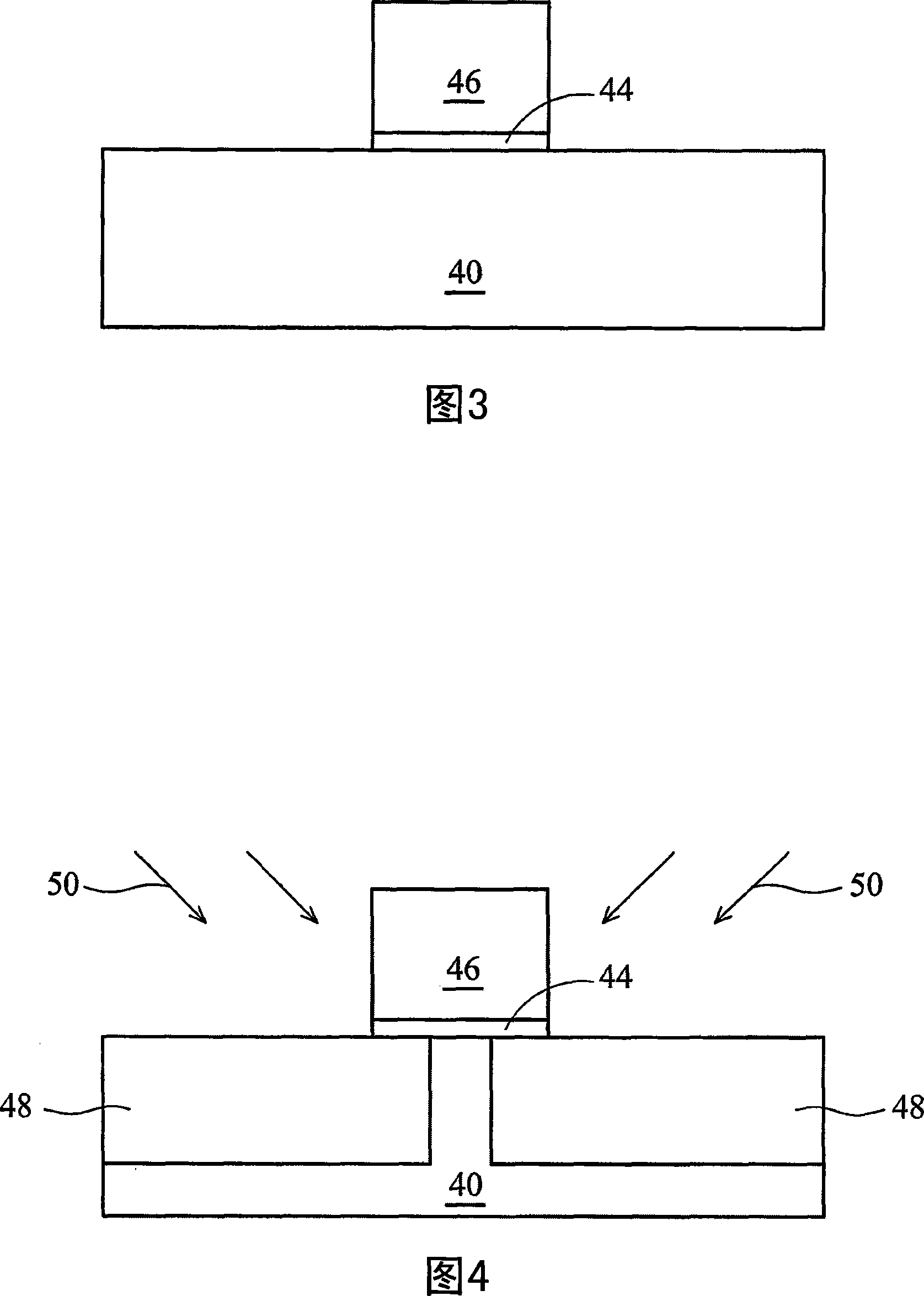
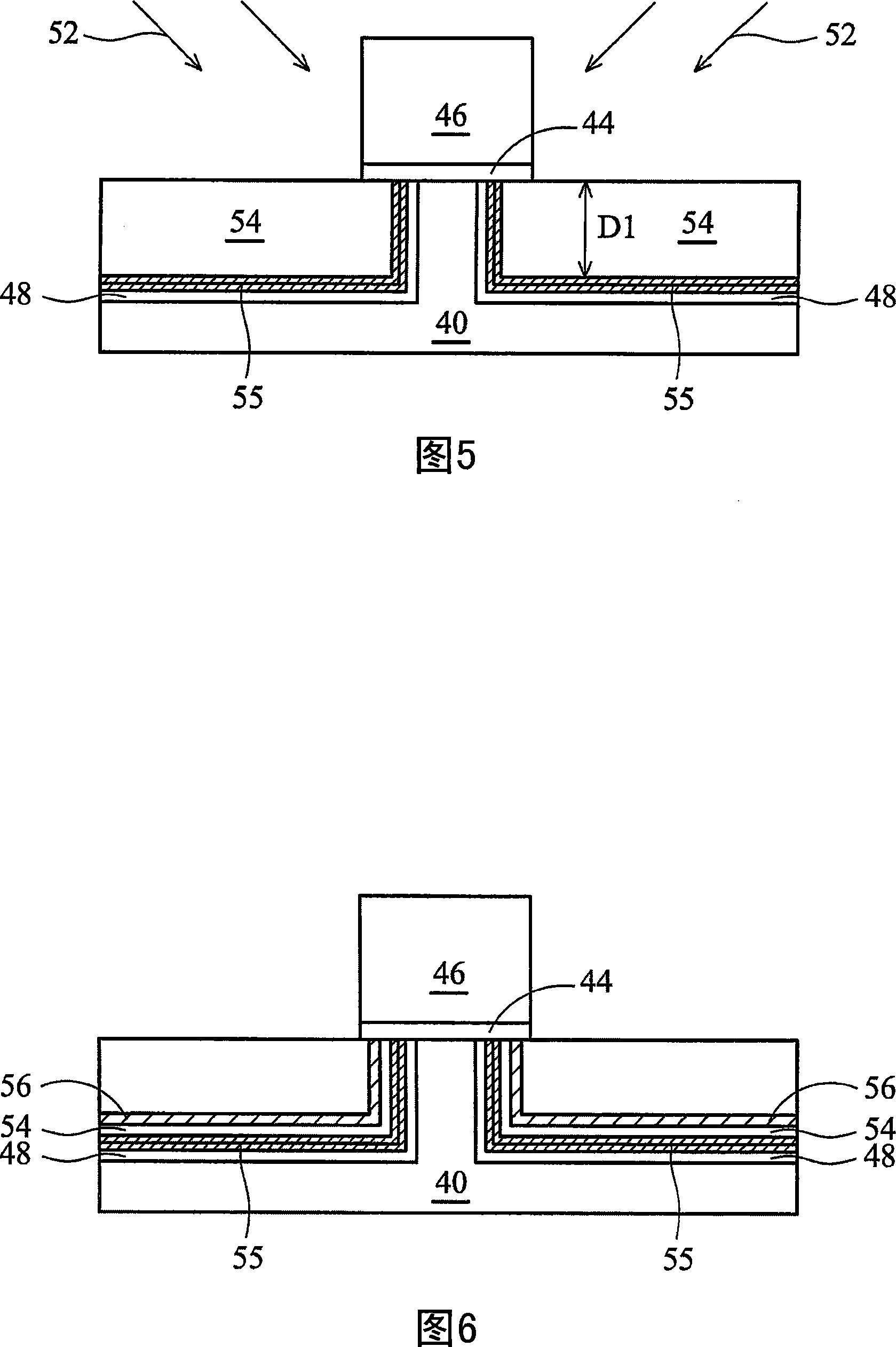
[0026] In high-performance NMOS devices, the source / drain regions preferably have low sheet resistance and shallow junctions. However, these two requirements are often contradictory. In order to reduce the sheet resistance, more activating impurities must be used, which will diffuse the impurities in the implanted region and increase the junction depth. In a preferred embodiment of the present invention, the impurity of the source / drain extension (also called lightly doped source / drain region, LDD region for short) is phosphorus. In the case of controlling the diffusion of phosphorus, the LDD region of the preferred embodiment of the present invention has a high concentration of phosphorus. 3-8C show process cross-sectional views of a preferred embodiment of the present invention. In different drawings, the same elements are labeled with the same reference numerals.
[0027] In FIG. 3, the gate dielectric layer 44 of the gate stack is formed on the substrate 40, and the gate 46 is...
PUM
 Abstract
Description
Claims
Application Information