Method of accelerating hot carrier injection investigating

A test method and hot carrier technology, applied in the direction of single semiconductor device testing, semiconductor/solid-state device testing/measurement, etc., can solve the problems of delaying data analysis time, taking a long time for MOS field effect device testing, speeding up speed limitations, etc. , to save time

Inactive Publication Date: 2007-12-19
SEMICON MFG INT (SHANGHAI) CORP +1
View PDF0 Cites 19 Cited by
  • Summary
  • Abstract
  • Description
  • Claims
  • Application Information

AI Technical Summary

Problems solved by technology

[0007] It can be seen that in the device failure experiment of hot carrier injection under accelerated stress conditions, the acceleration speed is still limited due to the limitation of the drain-source stress voltage selection, and the failure experiment cannot be performed eff

Method used


Image

  • Method of accelerating hot carrier injection investigating
  • Method of accelerating hot carrier injection investigating
  • Method of accelerating hot carrier injection investigating

Examples


Embodiment Construction

[0018] The present invention will be further described below with reference to the accompanying drawings and specific embodiments.

[0019] In one embodiment of the present invention, the present invention is briefly explained by taking an NMOS transistor as an example. First, measure the MOS hot carrier injection data at different temperatures according to the traditional method. During this process, measure the drain current Id and the substrate current Isub at different drain-source voltage Vds and gate-source voltage Vgs (maximum Isub bias) corresponding stress time. And set the 10% drain saturation current Idsat decay as the standard to get the stress time called failure time.

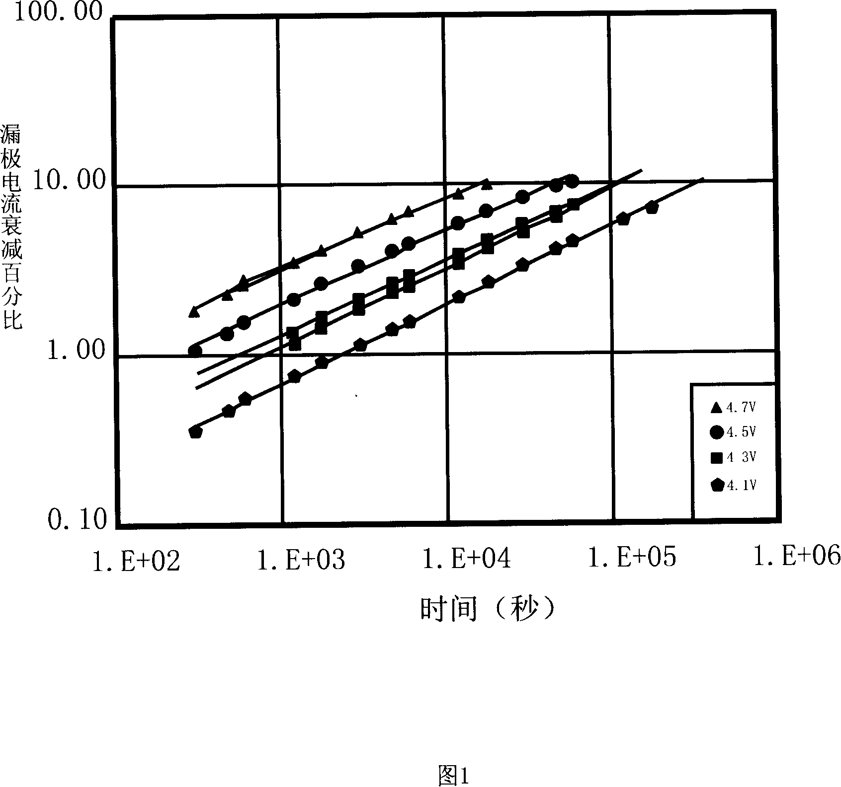
[0020] Please refer to FIG. 1 . FIG. 1 is a graph showing the relationship between drain saturation current decay and time for the NMOS transistor of the present invention at room temperature for different drain-source voltages. A typical device is used in this embodiment with a width to length ...


PUM


Abstract

A method for speeding up test of hot carrier injection includes separately measuring curve of drain electrode current and substrate current to time under different temperature and different bias voltage, setting failure condition and naming time realizing said failure condition to be failure time (FT), plotting out product of FT and drain electrode saturated current (DESC) and quotient of substrate current and DESC to obtain their relation, plotting out FT and temperature to obtain their relation and making low temperature failure test to derive out FT at the other temperature according to said relation of FT and temperature.

Description

Technical field [0001] The invention relates to the technical field of semiconductor testing, in particular to an accelerated hot carrier injection test for predicting the DC lifetime of a hot carrier MOS (Metal Oxide Semiconductor). Background technique [0002] At present, for the ultra-large-scale integrated circuit manufacturing industry, with the continuous reduction of the size of MOSFET (Metal Oxide Semiconductor Field Effect Transistor) devices, it has now been reduced to sub-micron and deep sub-micron, and is developing to ultra-deep sub-micron. While the size of the MOS device is proportionally reduced, the operating voltage of the device is not proportionally reduced, which greatly increases the formation probability of channel hot carriers, and generates interface states at the silicon-silicon dioxide interface, or is blocked by the gate. Charge trapping in the oxide layer leads to increased degradation of device characteristics such as threshold voltage, transco...

Claims


Application Information

Patent Timeline
IPC IPC(8): G01R31/26H01L21/66
Inventor 苏鼎杰邵芳耿静黄俊诚赵芳芳
Owner SEMICON MFG INT (SHANGHAI) CORP
Why Eureka
Try Eureka