Method for preparing single nano material in pore space structure

A technology of nanomaterials and holes, which is applied in the field of preparation of single nanomaterials, can solve the problems of expensive electron beam exposure process system and high process cost, and achieve the effect of controllable position, simple process and high efficiency

Inactive Publication Date: 2008-01-16
SUN YAT SEN UNIV
View PDF0 Cites 12 Cited by
  • Summary
  • Abstract
  • Description
  • Claims
  • Application Information

AI Technical Summary

Problems solved by technology

However, the electron beam exposure process system is extremely expensive, and the process cost is high

Method used


Image

  • Method for preparing single nano material in pore space structure
  • Method for preparing single nano material in pore space structure
  • Method for preparing single nano material in pore space structure

Examples


Embodiment Construction

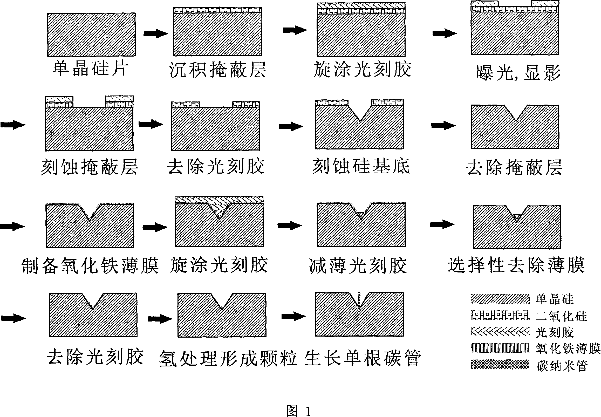
[0014] The present invention is a method of fabricating a single nanomaterial in a porous structure comprising the following sequential steps:

[0015] (a) Etch a hole structure on the substrate: first deposit a layer of masking layer on the substrate, then spin-coat a layer of photoresist, and use photolithography technology to open holes on the photoresist; The masking layer in the hole protected by the photoresist exposes the surface of the substrate, and then the photoresist is removed; the substrate material in the hole of the masking layer is etched to form a hole structure on the substrate, and then the masking layer on the surface is removed. The substrate can be metal, semiconductor or insulator, or a multi-layer structure material composed of two or more of the above materials as required. Etching adopts plasma etching or chemical solution etching.

[0016] (b) Depositing a metal or oxide film at the bottom of the hole in the substrate: first deposit a layer of meta...


PUM

PropertyMeasurementUnit
Thicknessaaaaaaaaaa

Abstract

The present invention relates to the preparation field of nanometer materials, disclosing a method for producing a single piece of nanometer material in a hole-shaped structure. First, a tiny hole is etched on a substrate, then metals or oxide films are positionally deposited on the bottom of the tiny hole, so that a single nanometer particle is formed in high-temperature annealing; or a single piece of one-dimensional nanometer material can be vegetated under the effects of metals or oxide films (such as catalytic action) through gas phase or liquid phase. The method has the advantages of simple technology and controllable location, which can realize the orientation growth of a single piece of nanometer material through controlling the position of the hole. The invention enables large-scale array type preparation with high efficiency.

Description

technical field [0001] The invention relates to the field of preparation of nanometer materials, in particular to a preparation method of a single nanometer material. Background technique [0002] A single nanomaterial, such as a single nanotube, a single nanowire, a single nanorod, and a single nanoparticle, has unique quantum size effects, ballistic transport effects, and superior photoelectric properties, so they will be used in the future High-performance nano-optoelectronic devices, such as light-emitting diodes, ultra-high-resolution flat panel displays, and high-sensitivity sensors, have potential application prospects. In order to facilitate the development of devices based on single nanomaterials, one of the first problems to be solved is to realize the localized preparation of single nanomaterials and their arrays. The methods of localized preparation of individual nanomaterials mainly include direct growth method, microtip welding method and solution dispersion m...

Claims


Application Information

Patent Timeline
IPC IPC(8): B82B3/00
Inventor 许宁生佘峻聪刘俊邓少芝陈军
Owner SUN YAT SEN UNIV
Why Eureka
Try Eureka