Plasma display panel and method for manufacturing the same

A display panel, plasma technology, applied in cold cathode manufacturing, electrode system manufacturing, discharge tube/lamp manufacturing, etc., can solve problems such as unavoidable impurities, high driving voltage of plasma display panels, fine cracks in protective layers, etc.

Inactive Publication Date: 2008-01-30
LG ELECTRONICS INC
View PDF3 Cites 4 Cited by
  • Summary
  • Abstract
  • Description
  • Claims
  • Application Information

AI Technical Summary

Problems solved by technology

However, the protective layer of a conventional plasma display panel cannot avoid impurities in its surface
Also, in a protective layer containing impurities, fine cracks may occur on the surface of the protective layer due to the impact caused by plasma particles
Cracks lead to reduced lifetime of the protective layer and may reduce the number of secondary electrons emitted from the protective layer during relative discharge
[0009] When the protective layer is only made of magnesium oxide, although the protective layer can increase the discharge coefficient of secondary electrons to a certain extent, the increase in the discharge coefficient is limited, and the resulting plasma display panel has a high driving voltage and low efficiency The problem

Method used


Image

  • Plasma display panel and method for manufacturing the same
  • Plasma display panel and method for manufacturing the same
  • Plasma display panel and method for manufacturing the same

Examples


Embodiment Construction

[0024] Reference will now be made in detail to the preferred embodiments of the present invention, examples of which are illustrated in the accompanying drawings. Wherever possible, the same reference numbers will be used throughout the drawings to refer to the same or like parts.

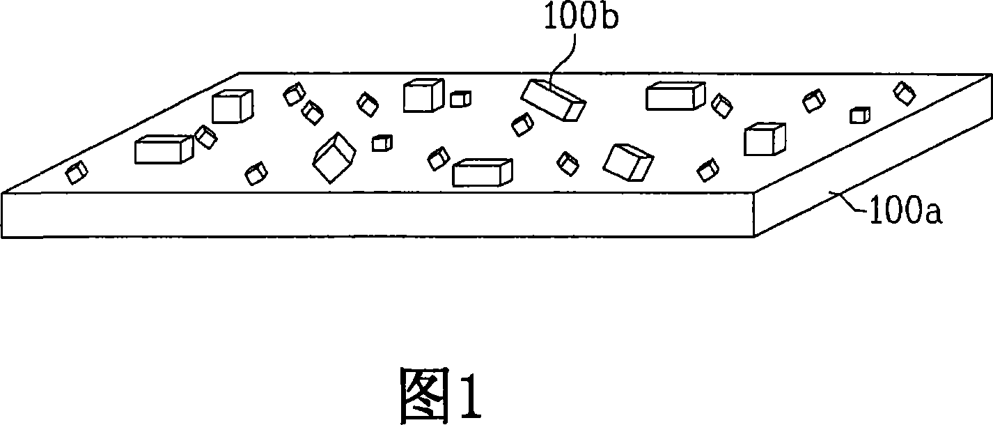
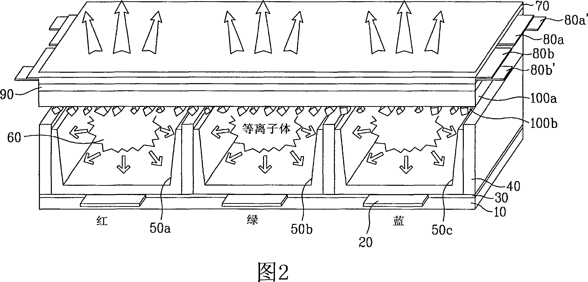
[0025] FIG. 1 is a view showing an example of the structure of a protective layer included in a plasma display panel according to the present invention. Now, a preferred embodiment of a protective layer included in a plasma display panel according to the present invention will be described with reference to FIG. 1 .

[0026] The first protective layer 100a is formed on a dielectric layer (not shown). The first protective layer 100a is made of magnesium oxide, and in addition, a dopant may be contained in the first protective layer 100a. The dopant has a function of improving discharge characteristics of secondary electrons included in the protective layer and reducing discharge delay. The dopant...


PUM

PropertyMeasurementUnit
sizeaaaaaaaaaa
thicknessaaaaaaaaaa
thicknessaaaaaaaaaa

Abstract

A protective layer, a protective layer manufacturing method of a plasma display panel, a plasma display panel, and a plasma display panel manufacturing method are provided to enhance emission characteristics of secondary electrons and to improve brightness and power consumption. A protective layer includes a first layer(280) and a second layer(280'). The first layer includes MgO. The second layer is formed on the first layer and includes a single crystalline metal oxide. The single crystalline metal oxide has a maximum value of cathode luminescence in a wavelength region of 300-500 nanometers. The single crystalline metal oxide is formed by supplying oxygen of 2-20sccm and argon of 0-18sccm in a gas state of a metal. The second layer is formed by coating irregularly particles including single crystalline metal powders on an entire surface of the first layer.

Description

[0001] The present invention claims Korean Patent Application No. 10-2006-0071601 filed on July 28, 2006, Korean Patent Application No. 10-2006-0071600 filed on July 28, 2006 and Korean Patent Application No. 10-2006-0071600 filed on July 28, 2006 and filed Korean Patent Application No. 10-2007-0008805, which are incorporated herein by reference. technical field [0002] The present invention relates to display devices, and more particularly, to protective layers and methods of manufacturing the same. Background technique [0003] With the advent of the multimedia age, there is an increasing demand for more refined and larger display devices capable of representing colors close to natural colors. Since existing cathode ray tubes (CRTs) have limitations in constructing large-size screens of 40 inches or more, liquid crystal displays (LCDs), plasma display panels (PDPs), projection televisions (TVs), etc. have expanded their use to The field of high-definition images has been...

Claims


Application Information

Patent Timeline
Patent Type & Authority Applications(China)
IPC IPC(8): H01J17/49H01J17/16H01J17/02H01J9/24H01J9/00H01J11/40
CPCH01J9/02H01J11/40
Inventor 金甫铉朴玟洙朴德海柳炳吉金泳成宋文奉赵元基
Owner LG ELECTRONICS INC
Why Eureka
Try Eureka