Semiconductor component and its making method

A manufacturing method and semiconductor technology, applied in the direction of semiconductor/solid-state device manufacturing, semiconductor devices, electrical components, etc., can solve the problems of complicated process and increase process cost, and achieve the effects of process simplification, accuracy improvement and cost saving

Active Publication Date: 2008-02-06
UNITED MICROELECTRONICS CORP
View PDF2 Cites 10 Cited by
  • Summary
  • Abstract
  • Description
  • Claims
  • Application Information

AI Technical Summary

Problems solved by technology

[0005] Since the use of PIP capacitors will add at least two photomask processes to the entire integrated circuit component process, such as the patterning of the polysilicon layer and the definition of the self-aligned metal silicide barrier layer, etc., all need to use the photomask process, so the process It is more complicated and will increase the process cost

Method used


Image

  • Semiconductor component and its making method
  • Semiconductor component and its making method
  • Semiconductor component and its making method

Examples


Embodiment Construction

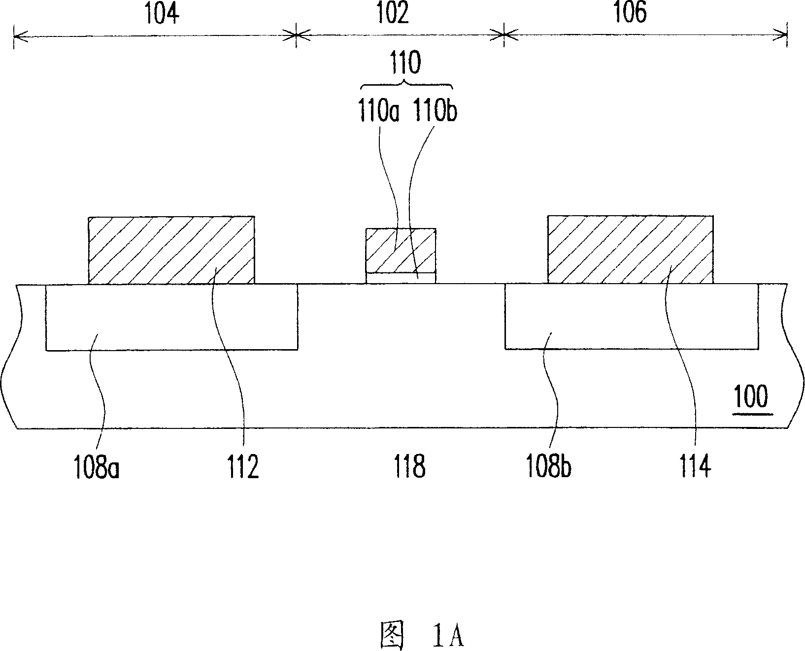
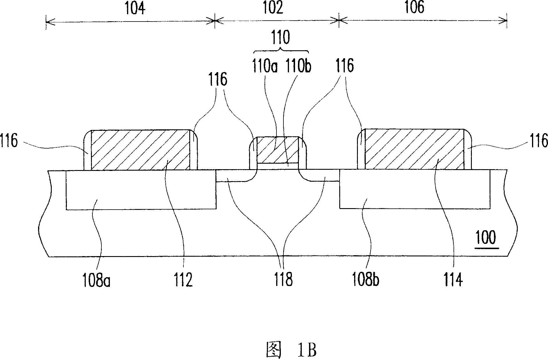
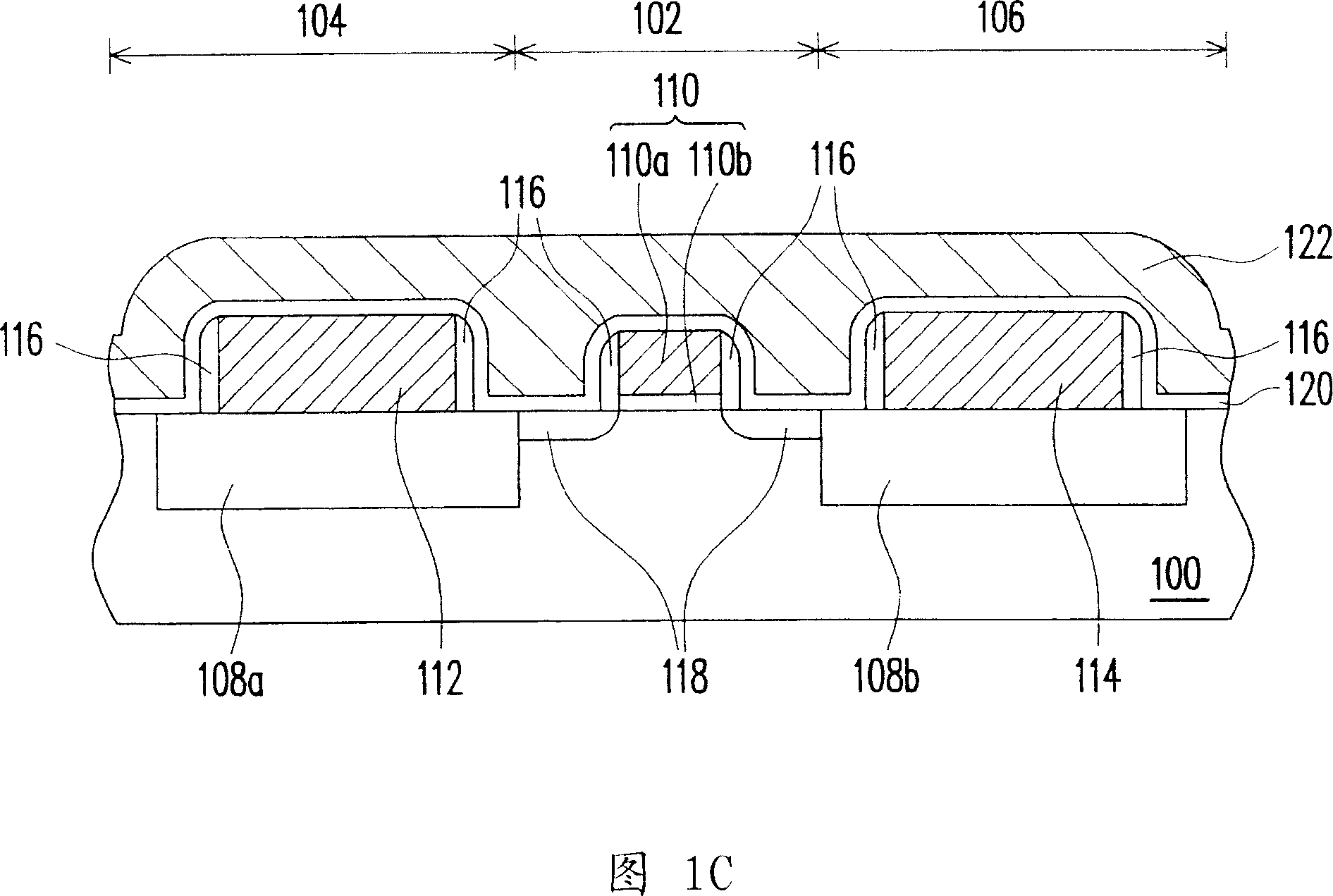
[0058] FIG. 1A to FIG. 1G are schematic cross-sectional flow diagrams of a manufacturing method of a semiconductor device according to an embodiment of the present invention.

[0059] First, referring to FIG. 1A , a substrate 100 is provided. The substrate 100 may be, for example, a silicon bulk substrate, and of course, the substrate 100 may also be, for example, a Silicon On Insulator (SOI) substrate. The substrate 100 has at least a transistor region 102 , a capacitor region 104 and a resistor region 106 . There is an isolation structure 108a in the substrate 100 of the capacitor region 104, and an isolation structure 108b is provided in the substrate 100 of the resistor region 106. The isolation structures 108a, 108b can be, for example, shallow trench isolation structures (STI), or in the form of Field isolation structures formed by local area oxidation technology (LOCOS).

[0060] 1A, a gate structure 110 is formed on the substrate 100 in the transistor region 102, an e...


PUM


Abstract

The present invention relates to a method for manufacturing semiconductor component. The method includes the step as follows: first providing a substrate which consists of a transistor area containing grid structure, a capacitor area containing an electrode 1 and a resistor area containing a resistor 2. Wherein, both the capacitor area and the resistor area comprise separating structure; then, forming in order a source electrode or drain electrode area amid a spacer 1 and both ends of the grid; afterwards, constituting a dielectric layer and a conductive material layer 1 above the substrate; and then patterning conductor layer 1 so as to form an electrode 3 of the capacitor area and a conductor layer of the resistor area; forming a spacer 2; removing uncovered dielectric layer; after that, conducting the technique of autoregistration type metal silicide and forming a layer of metal silicide with the aim to cover surface of the component.

Description

technical field [0001] The invention relates to a technology of an integrated circuit element, in particular to a semiconductor element and a manufacturing method thereof. Background technique [0002] Integrated circuits use various components to achieve desired circuit functions. These components may include bipolar and MOSFETs, junction diodes, resistors, and capacitors, among others. With the continuous development of electronic products, people's requirements for the properties of integrated circuits (Integrated Circuit, IC for short), such as high capacity, high efficiency, small volume, etc., are also constantly improving. [0003] For example, today's requirements for capacitors in the industry are that the capacitors can still have extremely high accuracy when no voltage is applied, that is, the capacitors must have good charge storage capabilities and minimize the phenomenon of charge loss. Among them, one of the types of capacitors widely used in the industry is...

Claims


Application Information

Patent Timeline
Patent Type & Authority Applications(China)
IPC IPC(8): H01L21/82H01L21/822H01L21/84H01L27/02H01L27/06H01L27/12
Inventor 高境鸿
Owner UNITED MICROELECTRONICS CORP
Why Eureka
Try Eureka