Semiconductor laser device and method for fabricating the same
一种激光装置、半导体的技术,应用在半导体激光器装置、半导体激光器、激光器装置等方向,能够解决无法保证信赖性等问题,达到降低导波路损失、简化制造工序的效果
Inactive Publication Date: 2010-12-01
PANASONIC CORP
View PDF1 Cites 0 Cited by
- Summary
- Abstract
- Description
- Claims
- Application Information
AI Technical Summary
Problems solved by technology
As a result, in the case of high output operation of 200mW or more, reliability cannot be guaranteed only by AR / HR coating (especially long-term reliability of thousands of hours or more)
Method used
View moreImage
Smart ImageViewing Examples

Examples
Embodiment Construction
Login to View More PUM
 Abstract
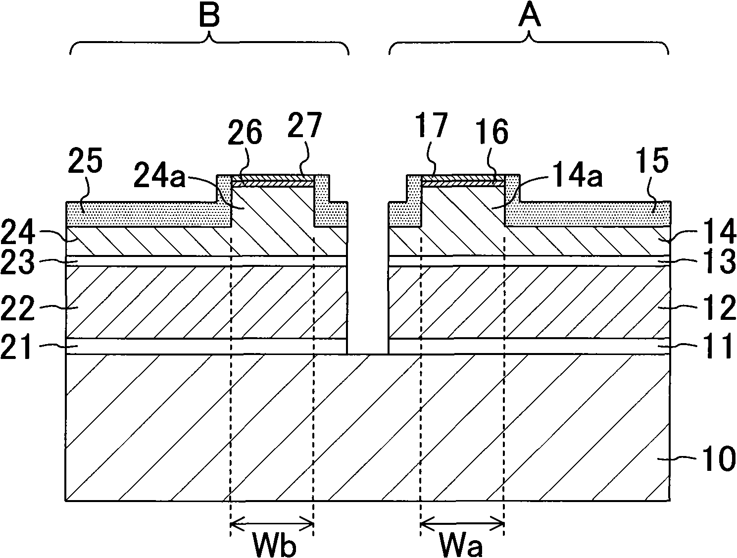
A semiconductor laser device includes a red-light-emission portion and an infrared-light-emission portion on a single substrate. The red-light-emission portion has a structure in which an AlGaInP-based active layer is sandwiched by a first cladding layer of a first conductivity type having a striped portion and a second cladding layer of a second conductivity type. The infrared-light-emission portion has a structure in which an AlGaAs-based active layer is sandwiched by a third cladding layer of the first conductivity type having a striped portion and a fourth cladding layer of the second conductivity type. The first, second, third, and fourth cladding layers are all made of an AlGaInP-based material. When in these layers, the Al:Ga contents are represented by X1:1-X1, X2:1-X2, X3:1-X3, and X4:1-X4, respectively, X1>=X2 and X3>=X4 are satisfied.
Description
Semiconductor laser device and manufacturing method thereof technical field The present invention relates to a semiconductor laser device, especially a light source for an optical head related to an optical disc device, and a semiconductor laser that emits light in a red region and an ultraviolet region as a light source in other electronic devices and information processing devices. Background technique Currently, a large-capacity digital video disc (DVD) capable of high-density recording and a digital video disc (DVD) device for recording and reproducing the same are commercially available, and are attracting attention as products whose demand will gradually increase in the future. Digital Video Disc (DVD) achieves high-density recording, so as a laser light source for recording and reproduction, AlGaInP series semiconductor lasers with an emission wavelength of 650nm are used. For this reason, the optical head of the digital video disc (DVD) device in the past is to uti...
Claims
Login to View More Application Information
Patent Timeline
 Patent Type & Authority Patents(China)
IPC IPC(8): H01S5/323H01S5/343H01S5/227H01S5/40H01S5/22
CPCH01S2301/18H01S5/221H01S5/4087H01S5/2218H01S5/162B82Y20/00H01S5/22H01S5/0287H01S5/34326H01S5/2201
Inventor 高山彻佐藤智也早川功一木户口勋
Owner PANASONIC CORP
Features
- R&D
- Intellectual Property
- Life Sciences
- Materials
- Tech Scout
- Unparalleled Data Quality
- Higher Quality Content
- 60% Fewer Hallucinations
Learn More Browse by: Latest US Patents, China's latest patents, Technical Efficacy Thesaurus, Application Domain, Technology Topic, Popular Technical Reports.
© 2025 PatSnap. All rights reserved.Legal|Privacy policy|Modern Slavery Act Transparency Statement|Sitemap|About US| Contact US: help@patsnap.com