Thin-film transistor LCD pixel structure and its making method

A liquid crystal display and thin film transistor technology, which is applied to the pixel structure of the thin film transistor liquid crystal display and its manufacturing field, can solve the problems of column spacer 12 sliding, white Mura, gate line dislocation, etc. The effect of great technological freedom

Active Publication Date: 2008-02-20
BEIJING BOE OPTOELECTRONCIS TECH CO LTD +1
View PDF0 Cites 10 Cited by
  • Summary
  • Abstract
  • Description
  • Claims
  • Application Information

AI Technical Summary

Problems solved by technology

[0006] Fig. 2 is a cross-sectional view of columnar spacers after the Cell process is completed. After the black matrix 13 and color filter 14 are formed on the color filter substrate, columnar spacers are formed below the black matrix 13 at positions corresponding to the TFT gate lines. Spacer 12, it can be seen from the figure that the columnar spacer 12 is supported on the insulating layer above the grid line, thereby maintaining the stability of the box thickness, but when the pressure is applied, the columnar spacer 12 will slide, resulting in black matrix 13 is misaligned with the grid line below, resulting in light leakage, that is, white Mura

Method used


Image

  • Thin-film transistor LCD pixel structure and its making method
  • Thin-film transistor LCD pixel structure and its making method
  • Thin-film transistor LCD pixel structure and its making method

Examples


Embodiment Construction

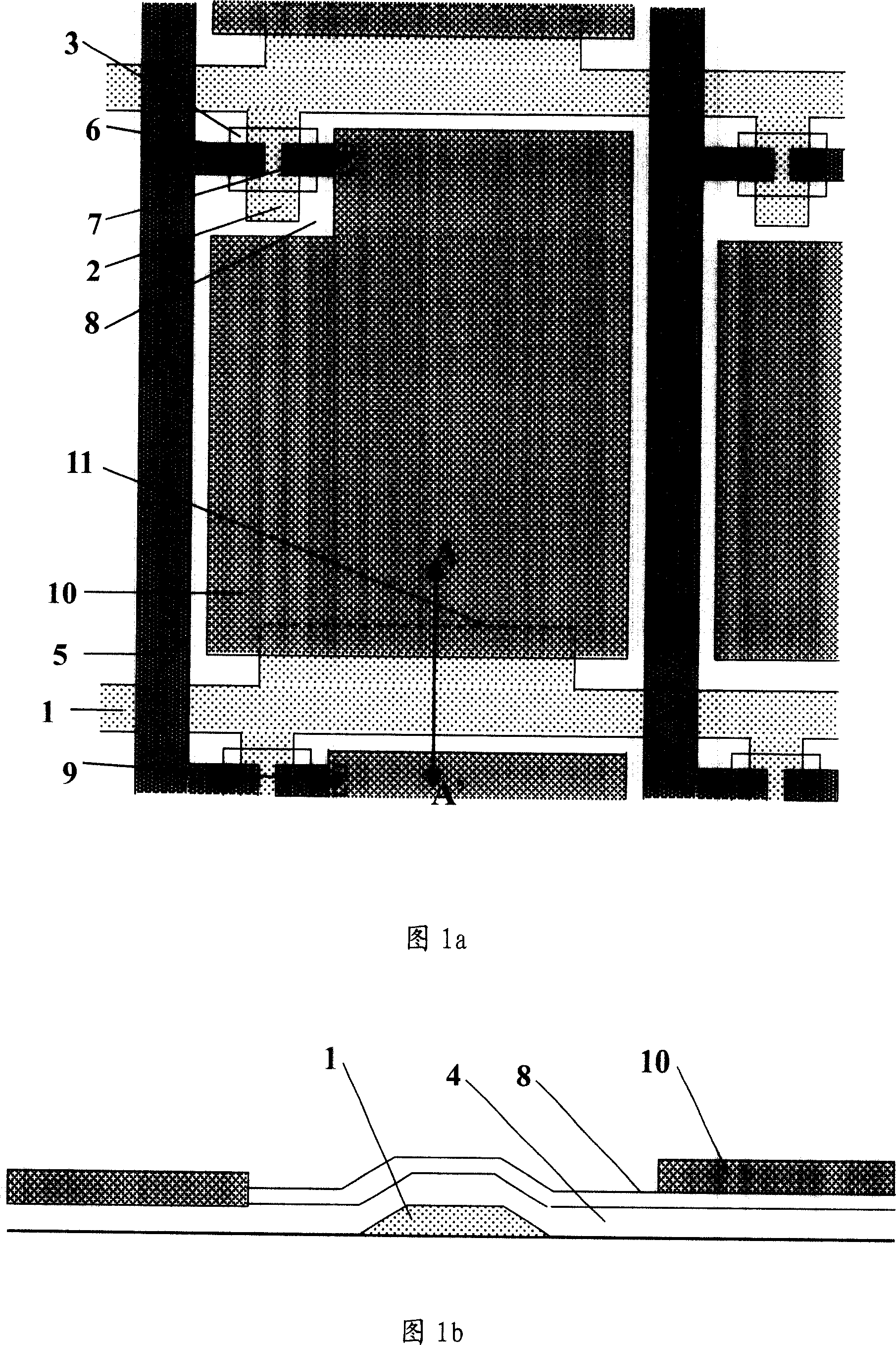
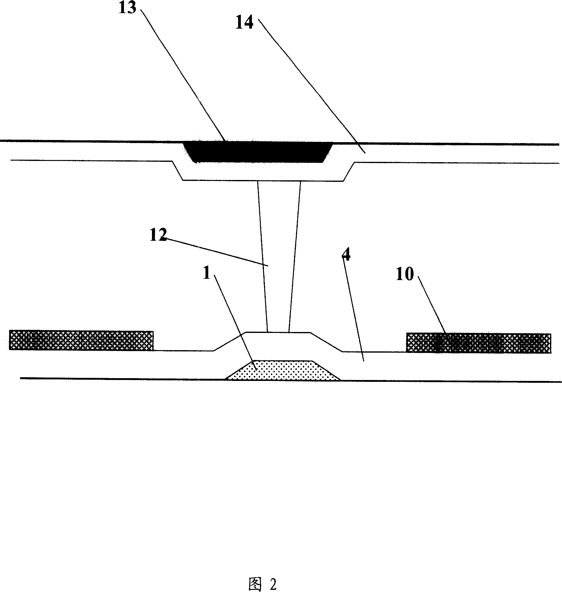
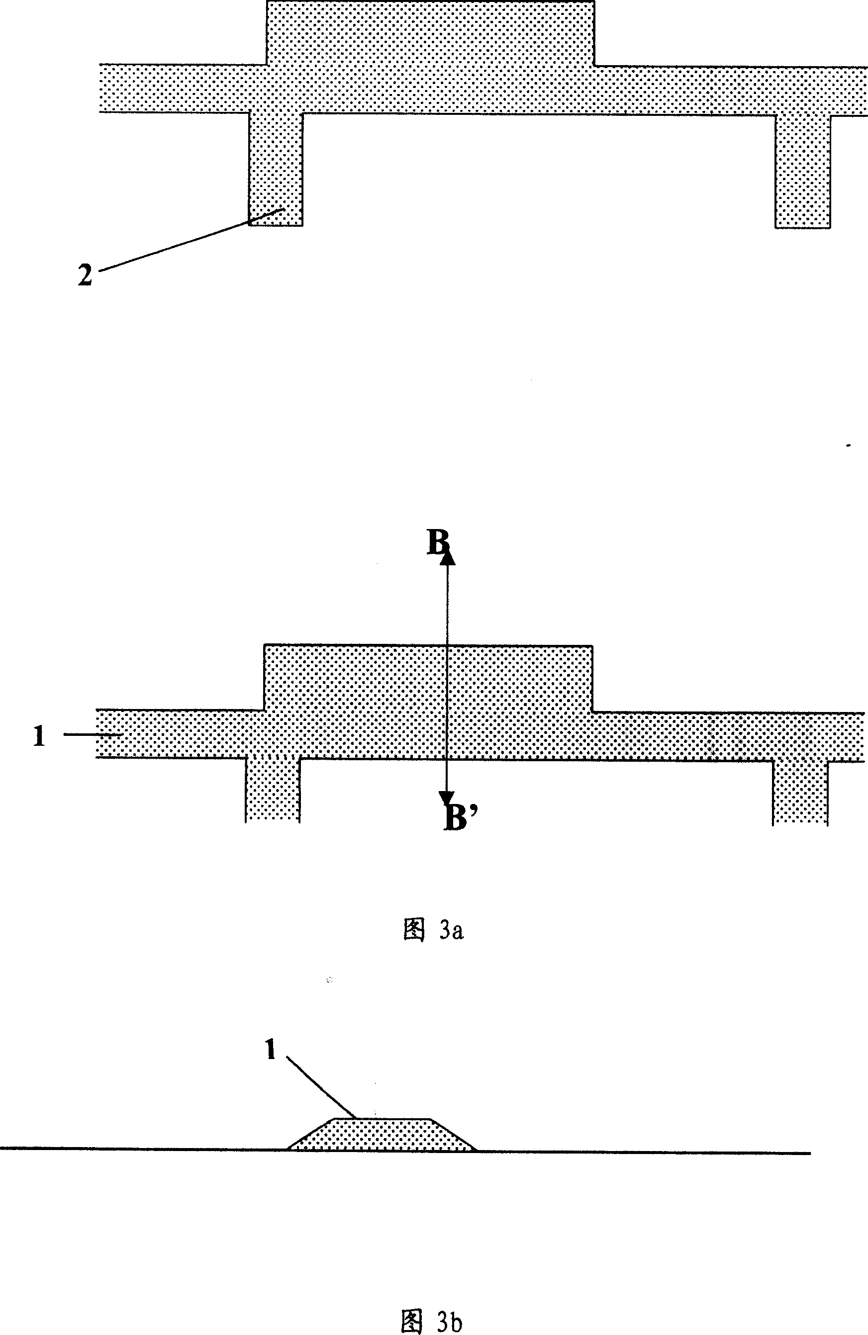
[0040] As shown in FIG. 7a, it is a planar structure diagram of a pixel in the present invention. The pixel structure includes: an insulating substrate; a gate line 1 and a gate electrode 2 formed on the insulating substrate; a gate insulating layer 4 formed on the gate electrode 2; a silicon island 3 formed on the gate insulating layer 4; The drain electrode 6 and the source electrode 7 above the island 3; the data line 5 and the drain electrode 6 of the source-drain electrode are integrated; the passivation layer 8 formed on the source-drain electrode covers the entire substrate; The passivation layer via hole 9; the pixel electrode 10 is connected to the source electrode 7 through the passivation layer via hole 9; the gate line protrusion 11 and the pixel electrode 10 together form a storage capacitor. These parts are not different from the prior art. The pixel structure is different from the prior art in that a hole 8a is formed on the gate insulating layer 4 and the passi...


PUM


Abstract

The utility model discloses an LCD pixel structure of a thin film transistor (TFT), which comprises a glass substrate, a plurality of grid lines, a grid electrode, a grid insulating layer, a silicon island, a source electrode, a leakage electrode, a plurality of data lines, a passivation layer and a pixel electrode. A hole is formed in the grid insulating layer and the passivation layer at the upper end of the grid lines, and a pixel electrode material layer is formed at the lower end of the hole. The utility model also discloses a manufacturing method of the thin film transistor (TFT) LCD pixel architecture, with the through hole forming in the pixel electrode, and also forming a matched hole with the columnar pad in shape and size at the upper end of the grid lines corresponding to the position of the columnar pad. The utility model has the advantages of effectively improving the phenomenon of white Mura comparing with the prior art, increasing the craft degree of freedom, reducing process defects, and improving the picture quality.

Description

technical field [0001] The invention relates to a thin-film transistor liquid crystal display (TFT LCD) pixel structure and a manufacturing method thereof, in particular to a thin-film transistor pixel structure and a manufacturing method for improving the phenomenon of white Mura (white inhomogeneity of picture quality). Background technique [0002] In recent years, with the popularization of digital TV, the traditional CRT display has tended to be replaced by a new generation of display technology due to its difficulty in digitization, large size, heavy weight, and radiation. The representative new display technology is PDP, OLED, LCD, etc. Among them, liquid crystal display (LCD) has begun to be widely popularized due to its advantages of light weight, thin volume, no radiation, low power consumption, and high display resolution, and has become a mainstream product. [0003] But the existing LCD technology still needs to be improved. In order to control the thickness o...

Claims


Application Information

Patent Timeline
Patent Type & Authority Applications(China)
IPC IPC(8): G02F1/136G02F1/1333G03F7/20
Inventor 陈旭
Owner BEIJING BOE OPTOELECTRONCIS TECH CO LTD
Why Eureka
Try Eureka