Method for measuring intra-cavity loss of LD pumping solid state laser device and equipment using the method
A solid-state laser, internal loss technology, applied in the field of lasers, can solve the problems of difficulty in guaranteeing reliability, affecting laser operation and laser output, complex structure, etc., to achieve the effect of non-interference measurement
- Summary
- Abstract
- Description
- Claims
- Application Information
AI Technical Summary
Problems solved by technology
Method used
Image
Examples
Embodiment 1
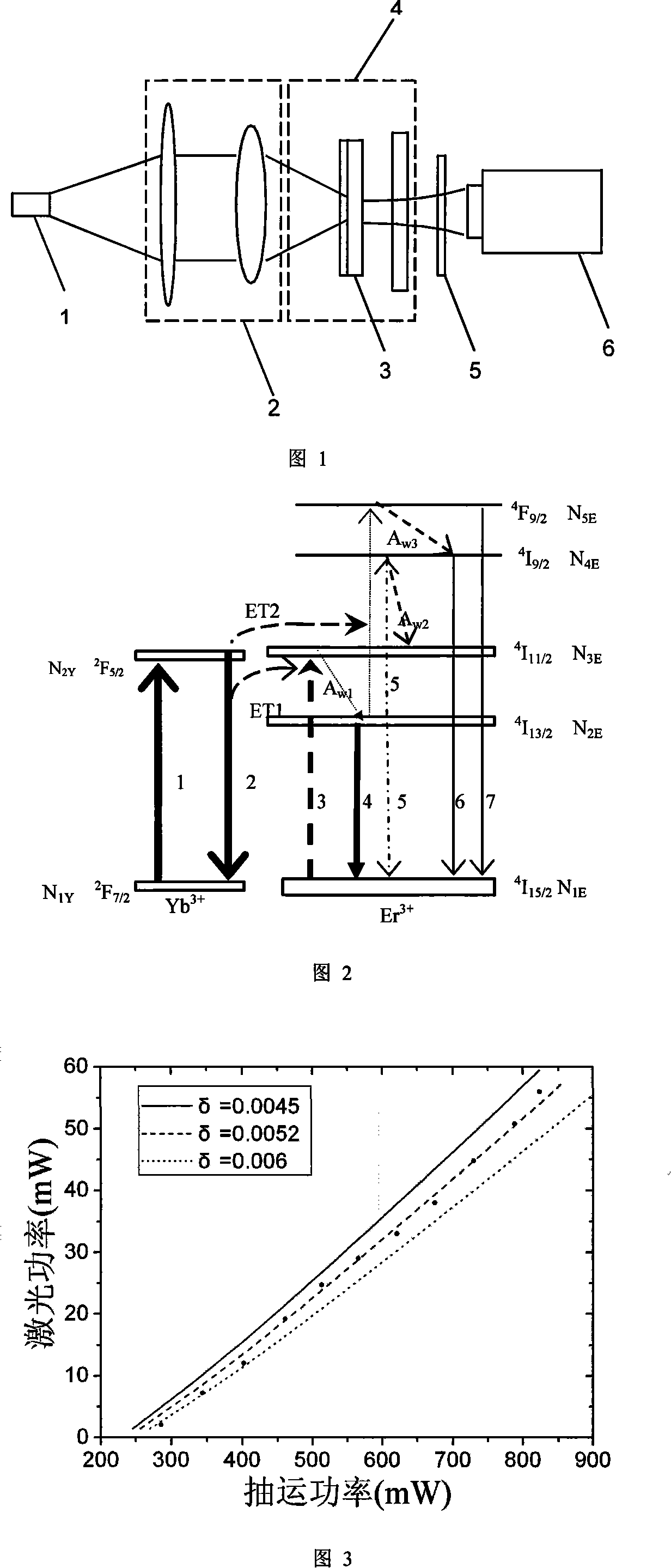
[0037] Embodiment 1: As shown in FIG. 1 , the implementation device of the present invention includes a pumping semiconductor laser 1 , a pump coupling system 2 , a laser medium 3 , a laser flat resonator 4 , a 975nm filter 5 , and a power meter 6 . The pumping light output by the pumping semiconductor laser 1 with a wavelength of 975nm passes through the pumping coupling system 2 and is coupled at the laser medium 3 into a circular light spot with a fundamental mode Gaussian distribution with a radius of 75 μm. The laser medium 3 is an erbium-ytterbium co-doped phosphate glass microchip with a thickness of 1 mm, and the concentration of erbium ions is N e 9.88×10 25 / cm 3 , Ytterbium ion concentration N Y 2.01×10 27 / cm 3 . The stimulated radiation of the laser medium 3 produces light with a wavelength of 1540nm, which is output as laser light after oscillating in the laser resonator cavity 4 . In this example, the total reflection mirror of the resonator cavity of the ...
Embodiment 2
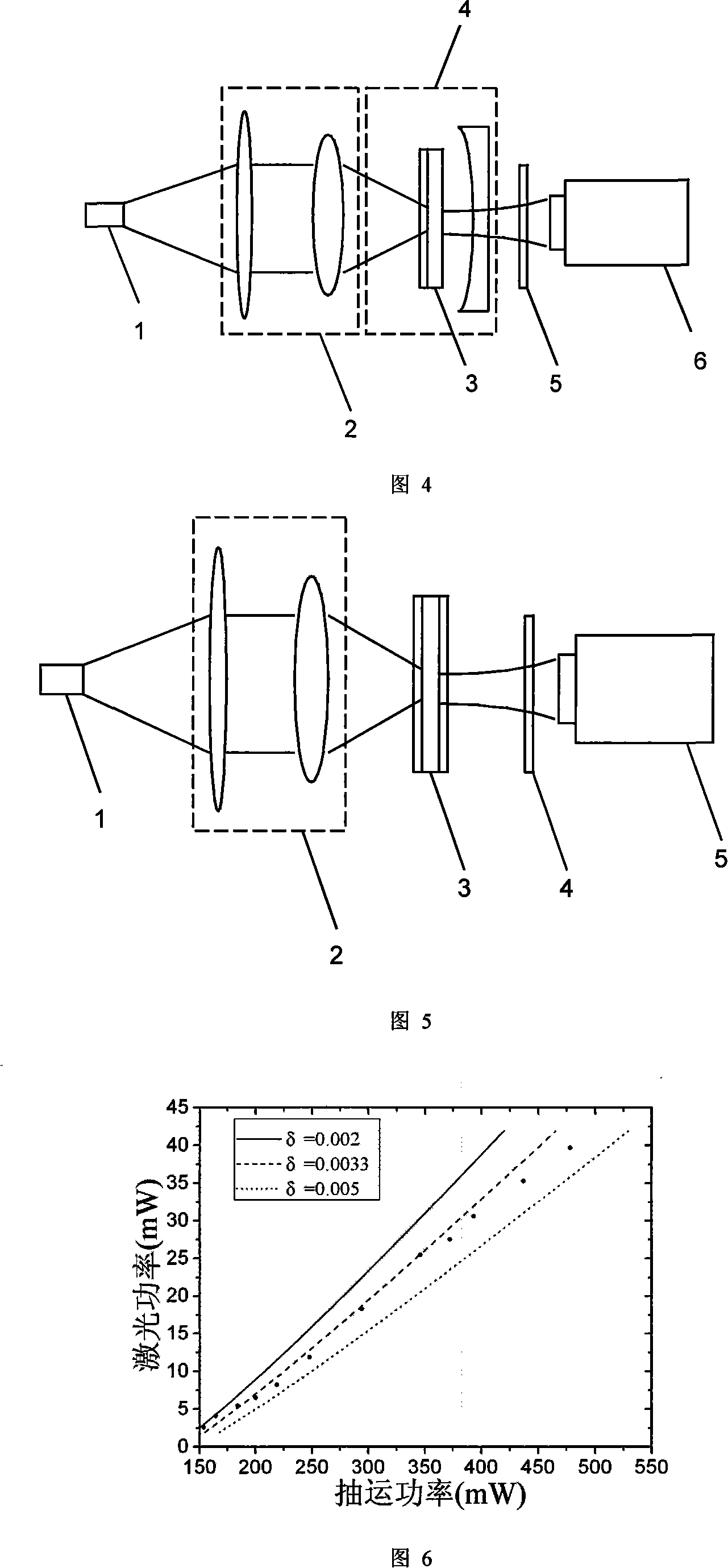
[0062] Embodiment 2: this embodiment is basically the same as Embodiment 1, and the difference is as shown in part 4 among Fig. 4, and the radius of curvature of the output mirror of the microchip laser cavity is 214mm, and the reflectivity is 99%, which is the same as that plated on the laser medium The 1540nm high-reflection film constitutes a flat-concave cavity, and its energy level and rate equation analysis are the same as those in Example 1. In the case of cavity lengths of 4.5, 5.5, and 6.5 mm, the round-trip losses in the flat-concave cavity are 0.0048, 0.0056, and 0.0059, respectively.
Embodiment 3
[0063] Embodiment 3: As shown in FIG. 5 , the implementation device of the present invention includes a pumping semiconductor laser 1 , a pumping coupling system 2 , a laser medium 3 , a 975nm filter 4 , and a power meter 5 . The pumping light output by the pumping semiconductor laser 1 with a wavelength of 975nm passes through the pumping coupling system 2 and is coupled at the laser medium 3 into a circular light spot with a fundamental mode Gaussian distribution with a radius of 75 μm. The laser medium 3 is an erbium-ytterbium co-doped phosphate glass microchip with a thickness of 1 mm, and the concentration of erbium ions is N e 9.88×10 25 / cm 3 , Ytterbium ion concentration N Y 2.01×10 27 / cm 3. The side of the laser medium 3 close to the pump coupling system 2 is coated with a total reflection film in the 1.54 μm band and an anti-reflection coating with a transmittance greater than 85% in the 0.98 μm band, and a coating with a transmittance of 1% in the 1.54 μm band...
PUM
 Abstract
Description
Claims
Application Information


