Flat wave-guide display apparatus panel
A waveguide display, flat technology, applied to instruments, identification devices, etc., can solve the problems of heat dissipation, low utilization rate of backlight, high precision requirements, etc., and achieve the effect of simple structure, rich colors, and pure three colors
- Summary
- Abstract
- Description
- Claims
- Application Information
AI Technical Summary
Problems solved by technology
Method used
Image
Examples
Embodiment 1
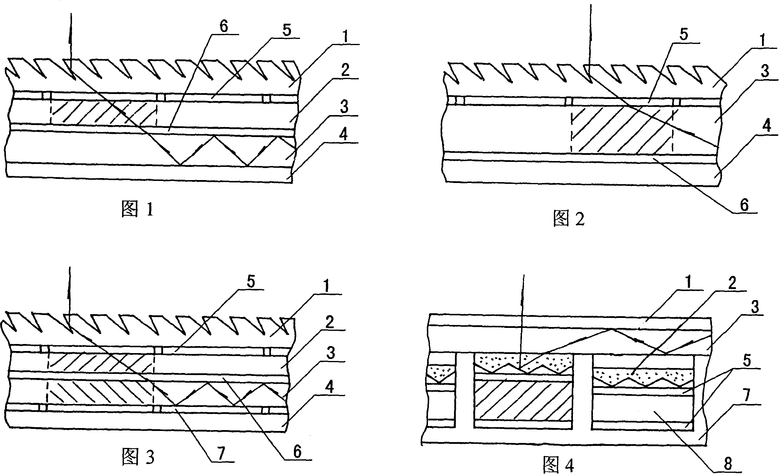
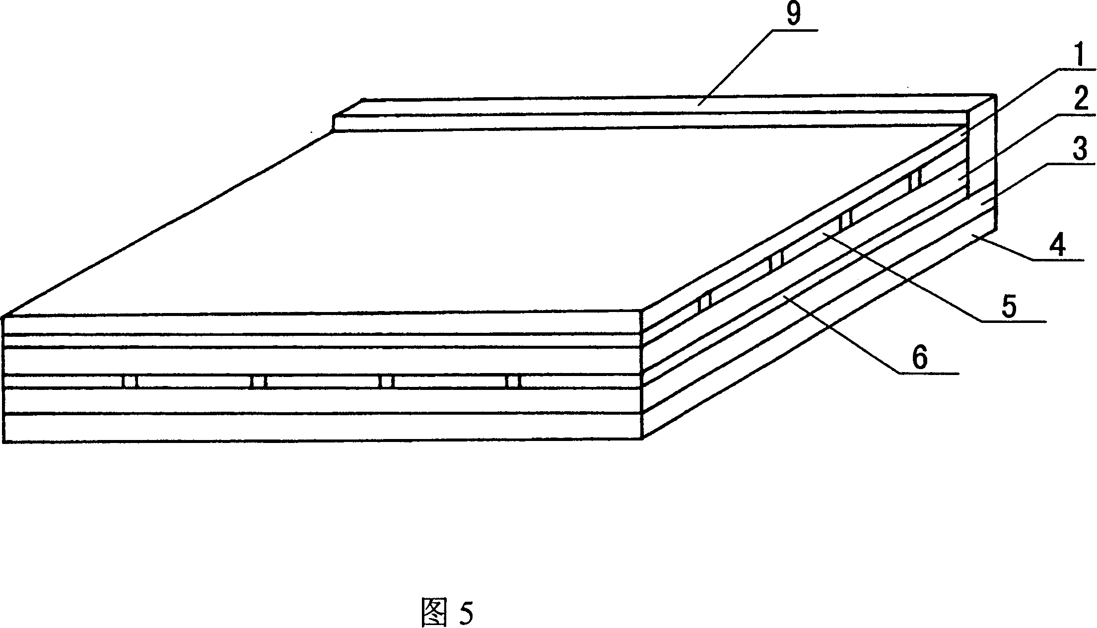
[0059] As shown in FIG. 5 , it is a structural schematic diagram of an electro-optic coupling flat waveguide display (1) according to an embodiment of the present invention; it includes a cover layer 1, an electro-optic coupling waveguide 2, a flat flat waveguide 3, a light source assembly 9 and a substrate 4; The electro-optical coupling waveguide 2 is located between the cover layer 1 and the flat plate waveguide 3; the substrate 4 is located on the other side of the flat plate waveguide 3; the selected flat plate waveguide 3 The refractive index is greater than the refractive index of the substrate 4 and the electro-optic coupling waveguide 2; a transparent scanning electrode 5 is arranged between the coupling waveguide 2 and the cover layer 1, and the coupling waveguide 2 and the flat plate-shaped waveguide 3 A transparent data electrode 6 is arranged between them; the covering layer 1 is a trapezoidal micro-prism transmission layer. The light source assembly 9 is located ...
Embodiment 2
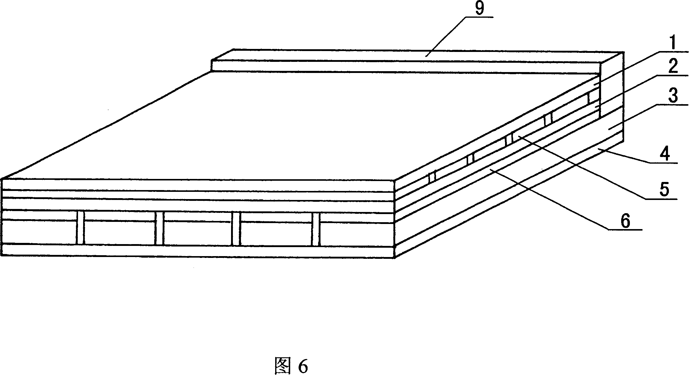
[0111] As shown in Figure 8, it is a structural schematic diagram of two strip-shaped electro-optic flat waveguide displays according to the embodiment of the present invention; the panel of the electro-optic flat waveguide display consists of micro-rib cover layer 1, ITO transparent scanning electrodes 5, and electro-optic strips from top to bottom. Shaped waveguide 3, data electrode 6, substrate 4. The ITO transparent scanning electrode 5 is located between the electro-optic strip waveguide 3 and the micro-rib covering layer 1 , and the data electrode 6 is located between the electro-optic strip waveguide 3 and the substrate 4 . The refractive index of the selected electro-optic strip waveguide 3 is greater than the refractive index of the micro-rib covering layer 1 and the substrate 4 ; and the refractive index of the selected micro-rib covering layer 1 is greater than that of the substrate 4 . The light source assembly 9 is located on one side of the display panel.
[011...
Embodiment 3
[0130] As shown in Figure 9, it is a structural schematic diagram of a three-electro-optical coupling bar-shaped electro-optic waveguide display in an embodiment of the present invention; 2. Transparent data electrodes 6 , electro-optic flat waveguides 3 , transparent scanning electrodes 7 and substrate 4 . The transparent scanning electrodes 5 are opposite to the transparent scanning electrodes 7 and have the same size. The refractive index of the selected electro-optical straight waveguide 3 is greater than the refractive index of the substrate 4 and the electro-optical coupling waveguide 2; the refractive index of the selected electro-optical coupling waveguide 2 is greater than the refractive index of the substrate 4; the covering layer 1 is a trapezoidal micro-prism transmission Floor. The light source assembly 9 is located on one side of the display panel.
[0131] 1. Panel production
[0132] 1. Substrate, scanning electrode, strip electro-optic flat waveguide and data...
PUM
 Abstract
Description
Claims
Application Information


