Epitaxial wafer and method of producing same

A technology of epitaxial wafers and manufacturing methods, which is applied in manufacturing tools, chemical instruments and methods, semiconductor/solid-state device manufacturing, etc. It can solve the problems of inability to measure LPD, large surface roughness, and reduce the amount of epitaxial layer polishing, etc., to achieve reduced detection The effect of critical size

Active Publication Date: 2010-06-09
SUMCO CORP
View PDF7 Cites 0 Cited by
  • Summary
  • Abstract
  • Description
  • Claims
  • Application Information

AI Technical Summary

Problems solved by technology

Therefore, the existing (110) crystal epitaxial wafers can only detect LPDs with a size of about 100 nm at most due to poor surface roughness. This is the current situation.
It is difficult to accurately detect LPD that is required to have a size of 100nm or less and exists on the main surface of a next-generation (110) crystal epitaxial wafer
[0008] If the amount of polishing after the formation of the epitaxial layer is increased, the thickness distribution on the wafer surface will become uneven and the flatness will be deteriorated, so it is not preferable.
On the other hand, if the amount of polishing after the formation of the epitaxial layer is reduced, the surface roughness will increase, and the detection critical dimension of LPD will exceed 100nm, making it impossible to measure small LPDs.

Method used


Image

  • Epitaxial wafer and method of producing same
  • Epitaxial wafer and method of producing same
  • Epitaxial wafer and method of producing same

Examples


Embodiment

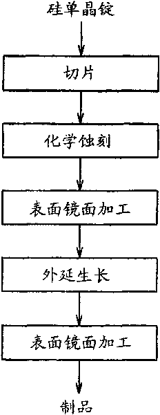
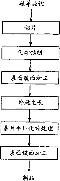
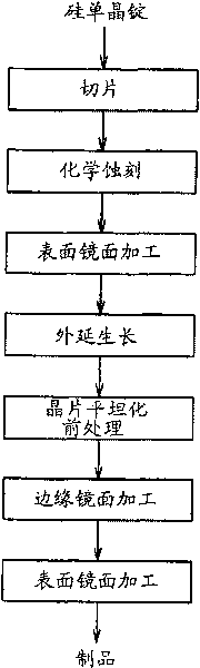
[0050] An embodiment is to slice a silicon single crystal ingot with a diameter of 305 nm to form a (110) wafer with a thickness of 900 μm. After the main surface of the sliced ​​wafer was chemically etched using an alkali solution, the surface and the back surface were subjected to mirror finishing by chemical polishing using colloidal silica. Next, 5% by volume of trichlorosilane (SiHCl 3 ), through decomposed silicon atoms, epitaxial growth of a single crystal silicon layer on a silicon wafer to form a 3 μm thick single crystal silicon layer. Next, a wafer planarization pretreatment process of immersing the wafer in a 5 ppm aqueous ozone solution at a temperature of 10 to 20°C for 1 to 10 minutes was performed to form a film with a thickness of 10 The oxide film was then subjected to surface mirror-finishing of the main surface of the wafer by chemical polishing using colloidal silica in a polishing amount of 0.2 μm, thereby manufacturing an epitaxial wafer.

[0051] For...


PUM

PropertyMeasurementUnit
sizeaaaaaaaaaa
critical dimensionaaaaaaaaaa
thicknessaaaaaaaaaa

Abstract

A method of producing an epitaxial wafer, comprising: performing epitaxial growth of silicon on a main surface of a wafer made of a silicon single crystal; performing surface flattening pretreatment of a main surface of the wafer using a treatment liquid of a predetermined composition at a temperature of 100 DEG C. or less, thereby forming an oxide film of a predetermined thickness while removingparticles adhered on the main surface of the wafer; and performing a surface polishing step where the main surface of the wafer is mirror polished.

Description

technical field [0001] The present invention relates to an epitaxial wafer and a manufacturing method thereof. Background technique [0002] Device substrates manufactured using silicon wafers tend to be miniaturized for reasons such as reduction of device costs. At the same time, the requirements for the surface roughness and flatness of wafers are becoming stricter year by year, and the reduction in size and number of LPDs (Light Point Defects) is also more required. [0003] The conventionally used silicon substrates are mainly manufactured using epitaxial wafers of (100) crystals (silicon wafers whose main surface is a (100) plane: adopting crystals of {100} wafers). However, in recent years, as a next-generation substrate suitable for use in MOSFETs (Metal Oxide Semiconductor Field Effect Transistors), MPUs of other MOS structure devices, logic arrays, etc., (110) (the main surface is a (110) plane) Silicon wafers: substrates made of epitaxial wafers (crystals of {110...

Claims


Application Information

Patent Timeline
Patent Type & Authority Patents(China)
IPC IPC(8): H01L21/205H01L21/30H01L21/306H01L21/31H01L21/304C30B33/00B28D5/00
CPCC30B29/06C30B23/02C30B33/005C30B25/02H01L21/20
Inventor 中原信司坂井正人土肥敬幸
Owner SUMCO CORP
Why Eureka
Try Eureka