Semiconductor device, embedded memory and manufacturing method thereof

An embedded memory and semiconductor technology, applied in semiconductor/solid-state device manufacturing, semiconductor devices, electric solid-state devices, etc., can solve problems such as adverse effects on output and process yield, potential yield reduction, etc., to improve process yield The effect of reducing the efficiency, reducing the cost of the process, and reducing the quantity required

Active Publication Date: 2008-03-12
TAIWAN SEMICON MFG CO LTD
View PDF0 Cites 8 Cited by
  • Summary
  • Abstract
  • Description
  • Claims
  • Application Information

AI Technical Summary

Problems solved by technology

[0004] Traditionally, the formation of MIM capacitors requires more than three layers of photomasks and complicated manufacturing processes, whic

Method used


Image

  • Semiconductor device, embedded memory and manufacturing method thereof
  • Semiconductor device, embedded memory and manufacturing method thereof
  • Semiconductor device, embedded memory and manufacturing method thereof

Examples


Example Embodiment

[0031] In order to make the above and other objects, features and advantages of the present invention more comprehensible, preferred embodiments are listed below and described in detail in conjunction with the accompanying drawings.

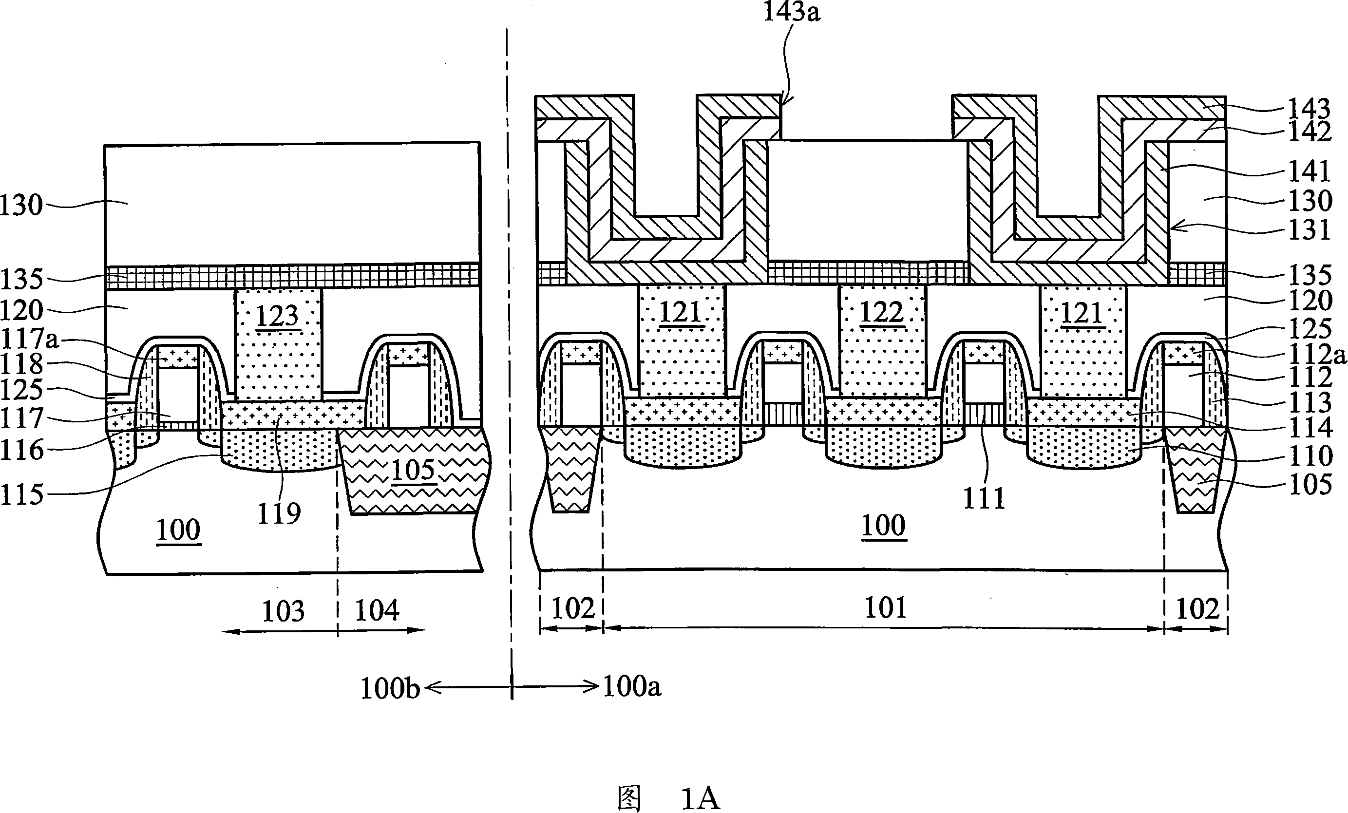
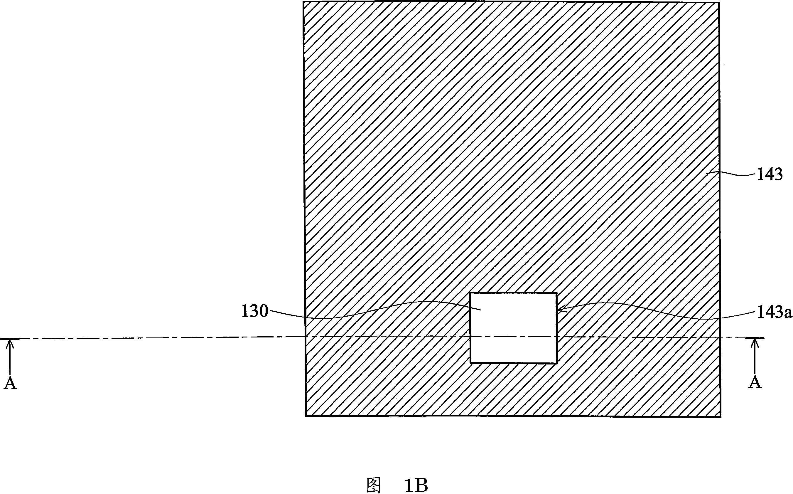
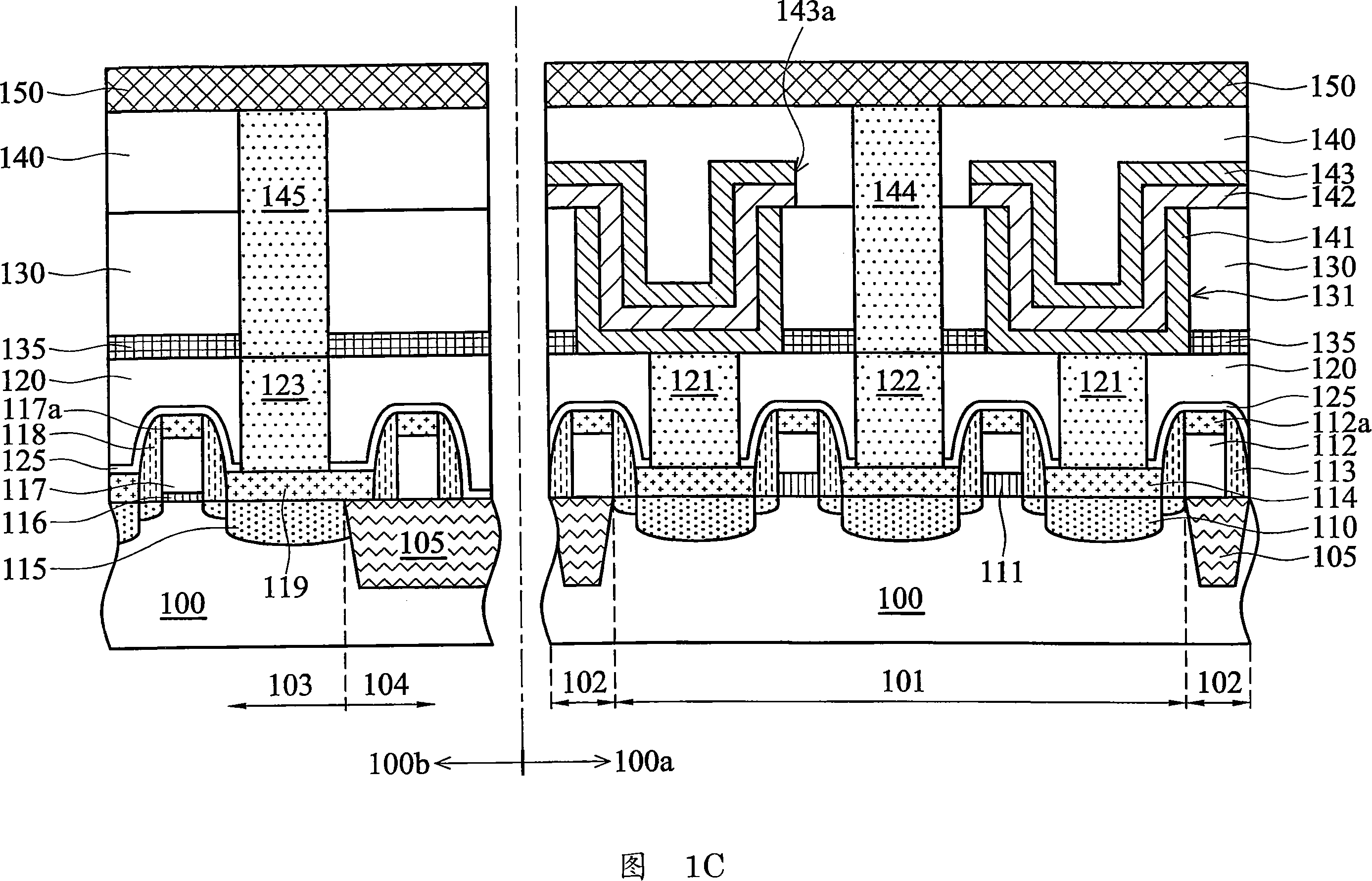
[0032]Please refer to FIG. 1A , which shows an embedded memory according to a preferred embodiment of the present invention, which includes a semiconductor device in a memory cell array (cellarray) region 100 a of a substrate 100 . The substrate 100 may include semiconductor materials, such as silicon, germanium, silicon germanium, compound semiconductors, or other semiconductor materials. The aforementioned semiconductor device includes a plurality of capacitors at least partially embedded in the interlayer dielectric layer 130 on the substrate 100 .

[0033] The interlayer dielectric layer 130 may comprise an organic dielectric, silicon oxide, or an oxide-based dielectric such as borophosphosilicate glass ( boron phosphate silicate glass (BPSG...


PUM

PropertyMeasurementUnit
Capacitanceaaaaaaaaaa

Abstract

Embedded memories. The devices include a substrate, a first dielectric layer, a second dielectric layer, a third dielectric layer, and a plurality of capacitors. The substrate comprises transistors. The first dielectric layer, embedding first and second conductive plugs electrically connecting the transistors therein, overlies the substrate. The second dielectric layer, comprising a plurality of capacitor openings exposing the first conductive plugs, overlies the first dielectric layer. The capacitors comprise a plurality of bottom plates, respectively disposed in the capacitor openings, electrically connecting the first conductive plugs, a plurality of capacitor dielectric layers respectively overlying the bottom plates, and a top plate, comprising a top plate opening, overlying the capacitor dielectric layers. The top plate opening exposes the second dielectric layer, and the top plate is shared by the capacitors.

Description

technical field [0001] The present invention relates to semiconductor technology, in particular to an embedded memory technology. Background technique [0002] Capacitors are widely used in semiconductor devices as elements for storing electrical charges. A capacitor essentially consists of two electrode plates separated by a dielectric material. The capacitance value or the amount of charge it can store under an applied unit voltage depends on many parameters, such as the area of ​​the electrode plates, the two electrodes The distance between the plates, and the dielectric constant of the dielectric material between the two electrode plates. Capacitors are used in filters, analog-to-digital converters, storage devices, controllers, and other kinds of semiconductor devices. [0003] A metal-insulator-metal (MIM) capacitor is one of many capacitors and is commonly used in mixed signal devices and logic devices such as embedded memories. MIM capacitors are used in various s...

Claims


Application Information

Patent Timeline
IPC IPC(8): H01L27/04H01L27/108H01L21/8242
CPCH01L27/0207H01L27/10894H01L27/10852H01L27/10897H10B12/033H10B12/50H10B12/09
Inventor 林宜经陈椿瑶王铨中伍寿国王中枢黄建华陈昆龙杨平
Owner TAIWAN SEMICON MFG CO LTD
Why Eureka
Try Eureka