Power LED with glue-filling formed bottom and manufacturing method thereof

A technology of LED chips and lenses, applied in electrical components, electric solid-state devices, circuits, etc., can solve the problems of restricting the development of such products, low production efficiency, etc., to meet the requirements of reflow soldering conditions, high product reliability, and increase adhesion the effect of strength

Active Publication Date: 2008-04-16
FOSHAN NATIONSTAR OPTOELECTRONICS CO LTD
View PDF1 Cites 48 Cited by
  • Summary
  • Abstract
  • Description
  • Claims
  • Application Information

AI Technical Summary

Problems solved by technology

The production efficiency of this lens preforming process is low, and due to the limitation of lens structure and material, the development of this type of product is greatly limited.

Method used


Image

  • Power LED with glue-filling formed bottom and manufacturing method thereof
  • Power LED with glue-filling formed bottom and manufacturing method thereof
  • Power LED with glue-filling formed bottom and manufacturing method thereof

Examples


Embodiment Construction

[0026] The concrete implementation examples of the present invention are described as follows:

[0027] 1. Lens forming mold preparation:

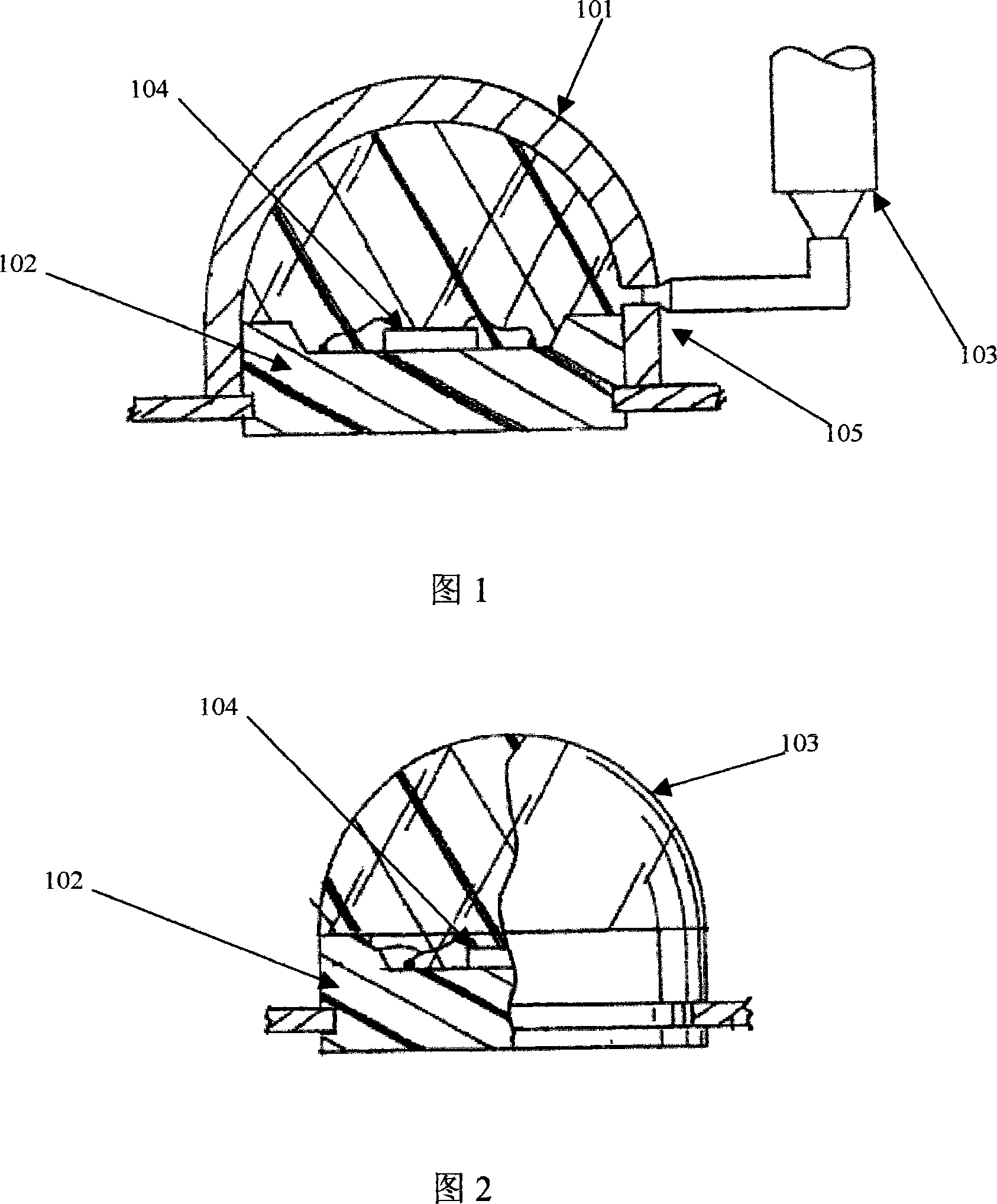
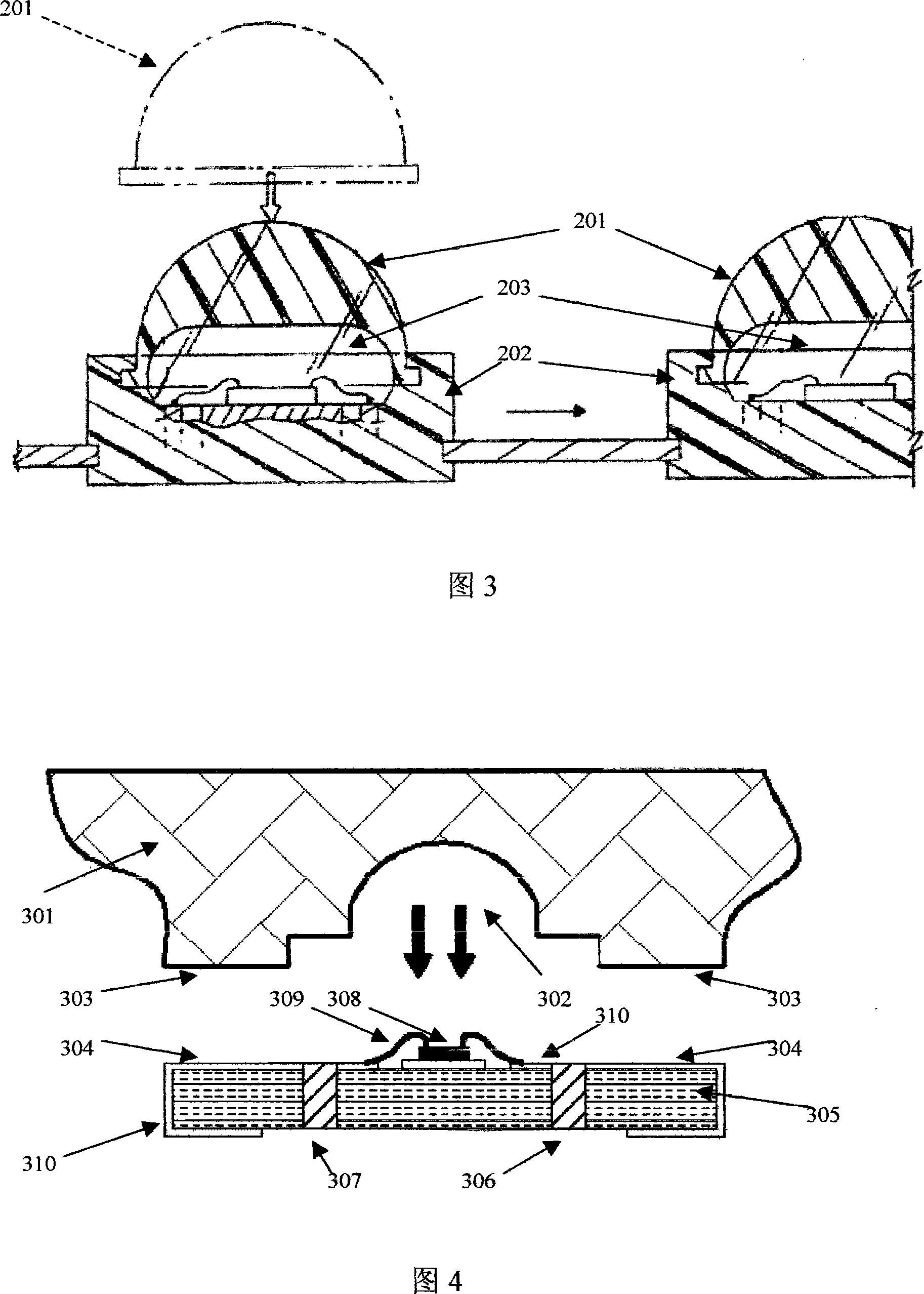
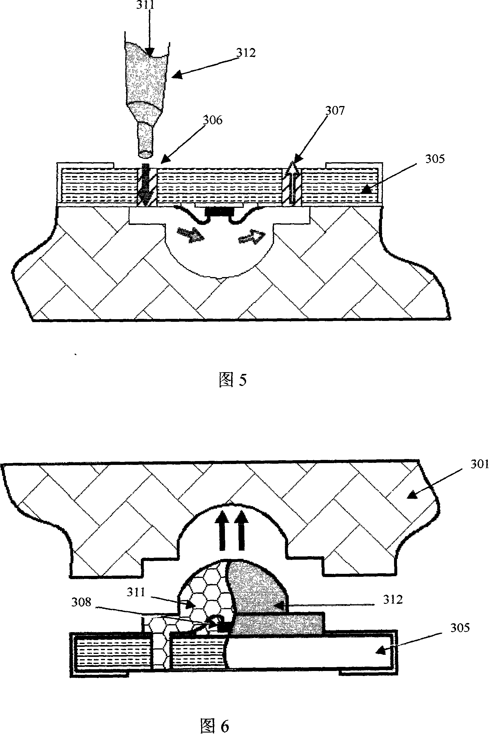
[0028] As shown in FIG. 4 , a cavity 302 conforming to the lens shape is prepared on one side of the material of the mold 301 , and the surroundings of the cavity 302 are kept flat to ensure sufficient contact between the contact surfaces 303 and 304 between the mold 301 and the substrate 305 .

[0029] 2. Substrate preparation:

[0030] The glue injection hole 306 and the exhaust hole 307 are processed on the substrate 305 by hole processing technology, as shown in FIG. 4 , the processing position is below the lens position, and the number is one each. The LED chip 308 is placed on the substrate 305 , and the electrode of the LED chip 308 is electrically connected to the lead electrode 310 on the substrate 305 by using the lead wire 309 through an ultrasonic welding process.

[0031] 3. Lamination of lens mold and substrate:

[0032] T...


PUM


Abstract

The present invention discloses a bottom plastic injection lens molding power LED and a method for manufacturing the same, and is characterized by comprising the following technique procedures: a plastic injection hole and an exhaust hole are arranged on a baseplate; an LED chip is arranged on the baseplate and after the electric connection is completed, a mould for lens molding is pressed on the baseplate; packaging colloid is injected to the plastic injection hole of the bottom of the baseplate; after the plastic injection is completed and the colloid is hardened, the module is taken off, thereby the packaging lens molding of the LED chip is completed. The colloid in the plastic injection hole and the exhaust hole of the invention increases the adhesive strengh of the packaging colloid on the baseplate; the invention has the advantages of convenient production technique and high reliability.

Description

technical field [0001] The patent of the present invention relates to a power light-emitting diode (LED) technology, in particular to a power LED formed by a bottom glue-injected lens and a manufacturing method thereof. The invention provides a light-emitting diode packaging technology with convenient manufacturing process and high reliability. Background technique [0002] The basic components of a current light-emitting diode (LED) include a substrate (frame), an LED chip, a lens formed by encapsulating colloid, and an inner lead. The inner lead connects the electrodes on the LED chip to the electrodes on the substrate to ensure that the external electrodes on the substrate deliver current to the LED chip; LED chips are semiconductor materials and are generally used in signal indication, display lighting and other fields because they can emit visible light. The main function of the encapsulation colloid is to protect the LED chip, export the light emitted by the LED chip,...

Claims


Application Information

Patent Timeline
Patent Type & Authority Applications(China)
IPC IPC(8): H01L33/00H01L33/48H01L33/52
CPCH01L33/52B29C45/14655H01L33/483H01L2224/48091
Inventor 余彬海李军政夏勋力
Owner FOSHAN NATIONSTAR OPTOELECTRONICS CO LTD
Why Eureka
Try Eureka