Check patentability & draft patents in minutes with Patsnap Eureka AI!

Resistor type memory element and manufacturing method thereof and operation method

A technology of resistive memory and operation method, applied in the direction of electrical components, static memory, read-only memory, etc.

Active Publication Date: 2008-04-16
MACRONIX INT CO LTD
View PDF0 Cites 1 Cited by
  • Summary
  • Abstract
  • Description
  • Claims
  • Application Information

AI Technical Summary

Problems solved by technology

The storage devices for accessing the above-mentioned digital products will also greatly increase the demand relatively speaking.

Method used


Image

  • Resistor type memory element and manufacturing method thereof and operation method
  • Resistor type memory element and manufacturing method thereof and operation method
  • Resistor type memory element and manufacturing method thereof and operation method

Examples


Embodiment Construction

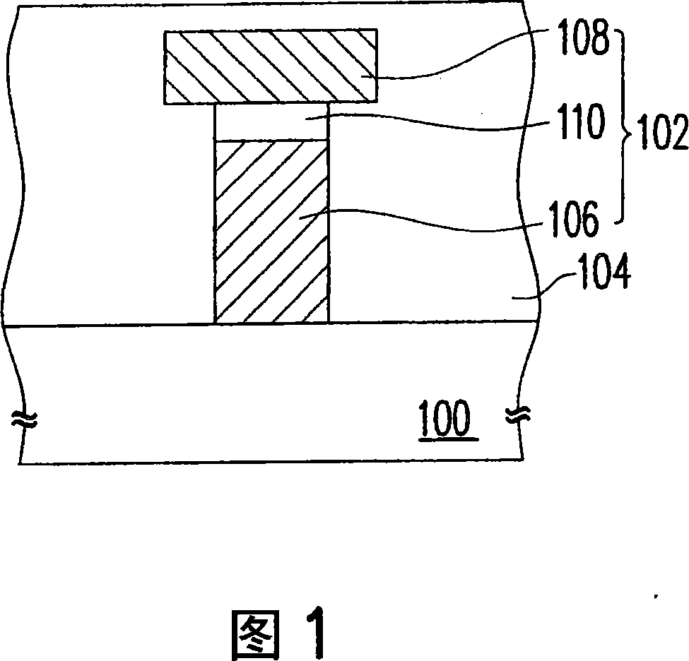
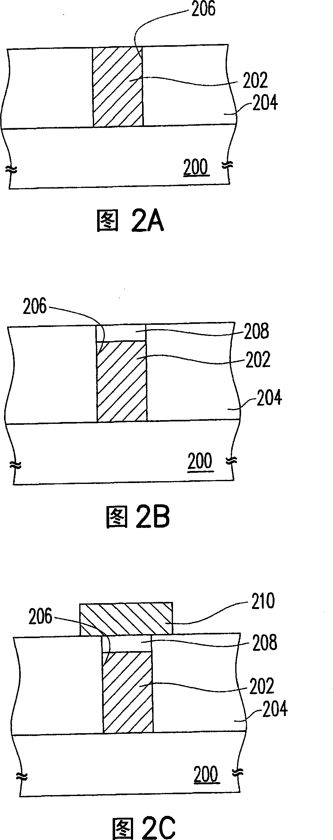
[0052] FIG. 1 is a cross-sectional view of a resistive memory device according to an embodiment of the present invention.

[0053] Referring to FIG. 1 , a resistive memory element 102 is disposed on a substrate 100 , and the resistive memory element 102 is disposed in a dielectric layer 104 on the substrate 100 , for example. The substrate 100 is, for example, a silicon substrate, and the material of the dielectric layer 104 is, for example, silicon oxide.

[0054] The resistive memory device 102 includes a tungsten electrode 106 , an upper electrode 108 and a tungsten oxide layer 110 .

[0055] The tungsten electrode 106 is disposed on the substrate 100 and used as a single electrode. The method of forming the tungsten electrode 106 is, for example, chemical vapor deposition.

[0056] The upper electrode 108 is disposed on the tungsten electrode 106 . The material of the upper electrode 108 is, for example, a semiconductor material such as doped polysilicon, or a metal mat...


PUM

PropertyMeasurementUnit
Thicknessaaaaaaaaaa

Abstract

A resistance type memory element is arranged on a substrate and comprises a tungsten electrode, an upper electrode and a tungsten oxide layer. The upper electrode is arranged on the tungsten electrode. The tungsten layer is arranged between the tungsten electrode and the upper electrode.

Description

technical field [0001] The present invention relates to a memory element and its manufacturing method and operating method, and in particular to a resistive memory element and its manufacturing method and operating method. Background technique [0002] Due to the development of communication technology and the rise of the Internet, people's demand for information exchange and processing has been accelerated, especially the demand for large-capacity audio-visual data transmission and fast transmission speed. On the other hand, in the face of global competition, the working environment has surpassed the office environment, and may need to go to a certain place in the world at any time. At this time, a large amount of information is needed to support its actions and decisions. Therefore, portable digital devices, such as: digital notebook computer / NB, personal digital assistant / PDA, e-book / e-Book, mobile phone / Mobile Phone, digital camera / DSC and other "Mobile Platforms (Mobile...

Claims


Application Information

Patent Timeline
IPC IPC(8): H01L45/00G11C11/56G11C16/10
Inventor 李明道何家骅赖二琨谢光宇
Owner MACRONIX INT CO LTD
Features
  • R&D
  • Intellectual Property
  • Life Sciences
  • Materials
  • Tech Scout
  • Unparalleled Data Quality
  • Higher Quality Content
  • 60% Fewer Hallucinations
Learn More