
Chip and its making method

A manufacturing method and semiconductor technology, applied in the direction of semiconductor/solid-state device manufacturing, electrical components, electrical solid-state devices, etc., can solve the problems of heavy labor costs, bump 920 bending, waste, etc., to improve product yield and increase structure The effect of strength, good structural strength

Active Publication Date: 2008-04-23
ADVANPAK SOLUTIONS PTE
View PDF0 Cites 8 Cited by
  • Summary
  • Abstract
  • Description
  • Claims
  • Application Information

AI Technical Summary

Problems solved by technology

[0005] However, during the process of assembling the semiconductor element 900 on the flip-chip mounting board, actions such as moving or alignment may easily cause the cylindrical bump 920 to bend (as shown in the rightmost bump in FIG. 1 and FIG. 2 ).
This makes it impossible for semiconductor components to be well assembled on flip-chip mounting boards, and even forms a short circuit, which affects the electrical function of the packaging structure
[0006] The above defective semiconductor element 900 is difficult to rework and repair, and must be disposed of as scrap
Even if defective semiconductor elements 900 can be reworked, expensive rework costs must be spent, which is quite wasteful
Therefore, a multi-channel defective product monitoring system is currently used in the process to avoid defective products from flowing into the next process and causing greater losses
However, this move must also result in an increase in process management costs

Method used


Image

  • Chip and its making method
  • Chip and its making method
  • Chip and its making method

Examples


no. 1 example

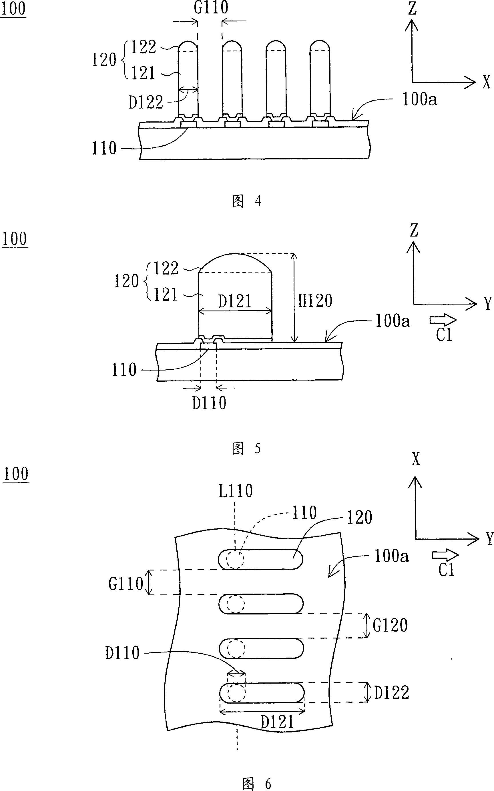
[0039] Please refer to Figures 4 to 6 at the same time. 4-5 are schematic side views of the semiconductor device 100 according to the first embodiment of the present invention, and FIG. 6 is a top view of the semiconductor device 100 in FIGS. 4-5. As shown in FIG. 4, the semiconductor element 100 has an active surface 100a. The semiconductor device 100 includes at least one pad 110 and at least one bump 120 . The welding pad 110 is disposed on the active surface 100 a and is a connecting structure for electrically connecting the active surface 100 a and the bump 120 . The bump 120 is vertically disposed on the pad 110 . As shown in Figure 6, the bump has a first diameter (Dimension) D121 and a second diameter D122 parallel to the active surface 100a (the first diameter D121 is shown in Figures 5 and 6, and the second diameter D122 shown in Figures 4 and 6). The first diameter D121 is greater than 1.2 times the second diameter D122. Because in this embodiment, the structur...

no. 2 example

[0064] The difference between the semiconductor device 200 and its manufacturing method in this embodiment and the semiconductor device 100 and its manufacturing method in the first embodiment lies in the disposition of bumps 220 , and the rest of the same parts will not be repeated here. Please refer to FIG. 11 , which shows a configuration diagram of the bumps 220 of the semiconductor device 200 according to the second embodiment of the present invention. In this embodiment, the semiconductor device 200 includes several bonding pads 110 and several bumps 220 . Each bump 220 corresponds to each pad 110 , and the directions C1 , C2 extending from the pads 110 of the bumps 220 are substantially parallel to each other. The pads 110 are arranged along the straight line L110 , and the bumps 220 alternately extend from the pads 110 toward opposite directions C1 , C2 to form a fan-shaped arrangement.

[0065] Therefore, there is a larger distance G220 between the protrusions 220 ex...

no. 3 example

[0069] The difference between the semiconductor device 300 and its manufacturing method in this embodiment and the semiconductor device 200 and its manufacturing method in the second embodiment lies in the structural design of the bump 320 , and the rest of the same parts will not be repeated here. Please refer to FIG. 12 , which shows a configuration diagram of the bumps 320 of the semiconductor device 300 according to the third embodiment of the present invention. In this embodiment, the bump 320 of the semiconductor device 300 has a cross section parallel to the active surface 300a, and the cross section is substantially a T-shaped structure.

[0070] As shown in FIG. 12 , the substantially T-shaped bump 320 extends a first distance D31 from the pad 110 toward a first direction C31 , and then extends a second distance D32 toward a second direction C32 and a third direction C33 respectively. The first distance D31 is greater than 1.2 times the width D110 of the pad 110 .


PUM


Abstract

The semiconductor component comprises at least coupling member whose maximal diameter is less than 100 micron and one lug bulge. The coupling member is located on the driving surface. The bulge is located on the coupling member in order to make the coupling member to electrically connect to the driving surface. The bulge comprises a cylinder part and a top part; the cylinder part is located on the coupling member; the top part is located on the top of the cylinder part; the cylinder part has a first diameter length and a second diameter length parallel to the driving surface; the first diameter length is 1.2 times longer than the second diameter length.

Description

technical field [0001] The present invention relates to a semiconductor element and its manufacturing method, and in particular to a standard fine-pitch semiconductor element and its manufacturing method. Background technique [0002] Modern technology is changing with each passing day, and various electronic products are constantly being introduced. With the widespread use of electronic products in daily life, the demand for semiconductor components is increasing day by day. As the design of semiconductor components is becoming lighter and thinner, when the size of semiconductor components shrinks, the number of I / Os increases instead of decreasing, which reduces the line pitch (Pitch) and line width. In order to solve this problem, the industry has developed a standard fine pitch (FinePitch) technology. [0003] Please refer to Figures 1 to 3 at the same time. 1-2 are schematic side views of a conventional semiconductor device 900 , and FIG. 3 is a top view of the semic...

Claims


Application Information

Patent Timeline
Patent Type & Authority Applications(China)
IPC IPC(8): H01L23/485H01L21/60
CPCH01L24/11H01L2224/11H01L2924/00012
Inventor 周辉星王志坚
Owner ADVANPAK SOLUTIONS PTE
Learn More