Photo-etching illumination system

A lighting system and lithography technology, applied in the field of micro-lithography, can solve the problems of reducing the transmittance of the lighting system, increasing the complexity of the system structure, etc., achieving continuously adjustable lighting coherence, avoiding energy loss, and improving stability Effect

Active Publication Date: 2008-05-07
SHANGHAI MICRO ELECTRONICS EQUIP (GRP) CO LTD
View PDF1 Cites 30 Cited by
  • Summary
  • Abstract
  • Description
  • Claims
  • Application Information

AI Technical Summary

Problems solved by technology

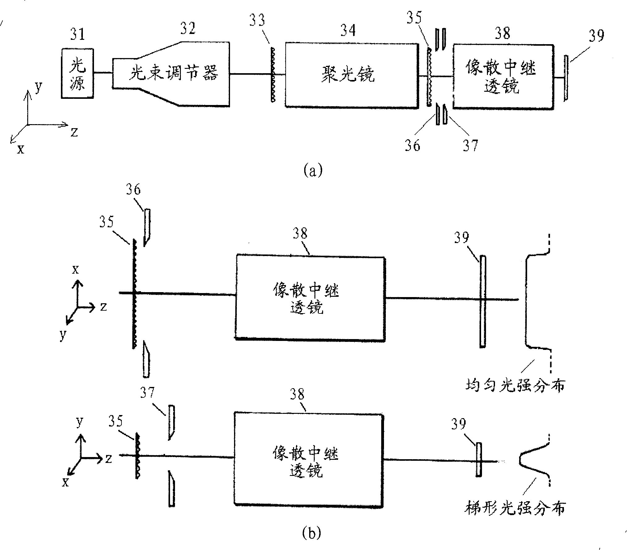
[0007] A major disadvantage of the above-mentioned lighting system is that a relay lens 38 must be used to obtain a continuously adjustable one-dimensional trapezoidal ligh

Method used


Image

  • Photo-etching illumination system
  • Photo-etching illumination system
  • Photo-etching illumination system

Examples


Embodiment Construction

[0052] The lithography illumination system of the present invention will be further described in detail below, and the "axis" referred to in the following all refers to the direction along the optical axis.

[0053] Such as Figure 4 As shown, the lithography illumination system of the present invention includes in turn from the object side to the image side: a light source 100 for generating an illumination beam of a specific wavelength, such as: 248nm, 193nm, 157nm, 126nm, etc.; a pupil shaping module 200 for receiving The illumination beam from the light source 100 forms an illumination beam with a specific cross-sectional shape; the microlens array module 300 receives the illumination beam from the pupil shaping module 200 and forms an illumination beam with a one-dimensional trapezoidal light intensity distribution; and the condenser lens 400, The illuminating light beam from the microlens array module 300 is received, and the condensed illuminating light beam is projecte...


PUM

PropertyMeasurementUnit
Wavelengthaaaaaaaaaa

Abstract

The invention provides a photoetching lighting system for semiconductor photoetching machine, comprising a light source, a pupil shaping module, a lenticule array module and a light condenser, wherein, the light source is used to generate lighting beam; the pupil shaping module is used to receive the lighting beam generated by the light source and form the lighting beam into cross section with specified shape; the lenticule array module is used to receive the lighting beam from the pupil shaping module and form the lighting beam with one-dimensional trapezoid light intensity distribution lighting beam; the light condenser is used to receive the lighting beam from the lenticule array module and project the converged lighting into a lighting field; the lenticule array module comprises at least two lenticule arrays and two pairs of edge arrays. The invention has the advantages of simple structure, high transmittance, ability to generate trapezoid light intensity distribution lighting field, and applicability to photoetching machine with the wavelength of 248nm, 193nm or other wavelengths.

Description

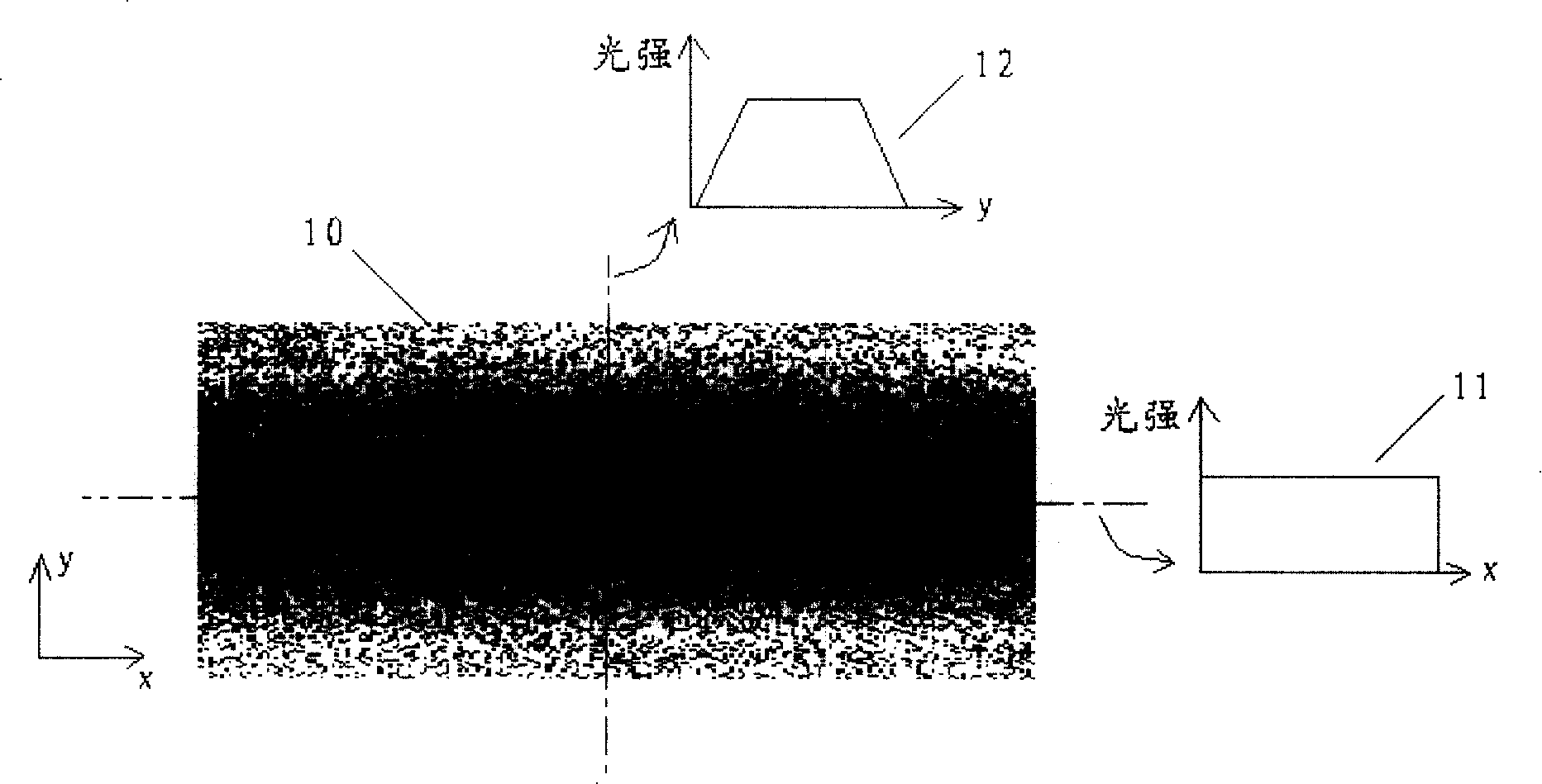
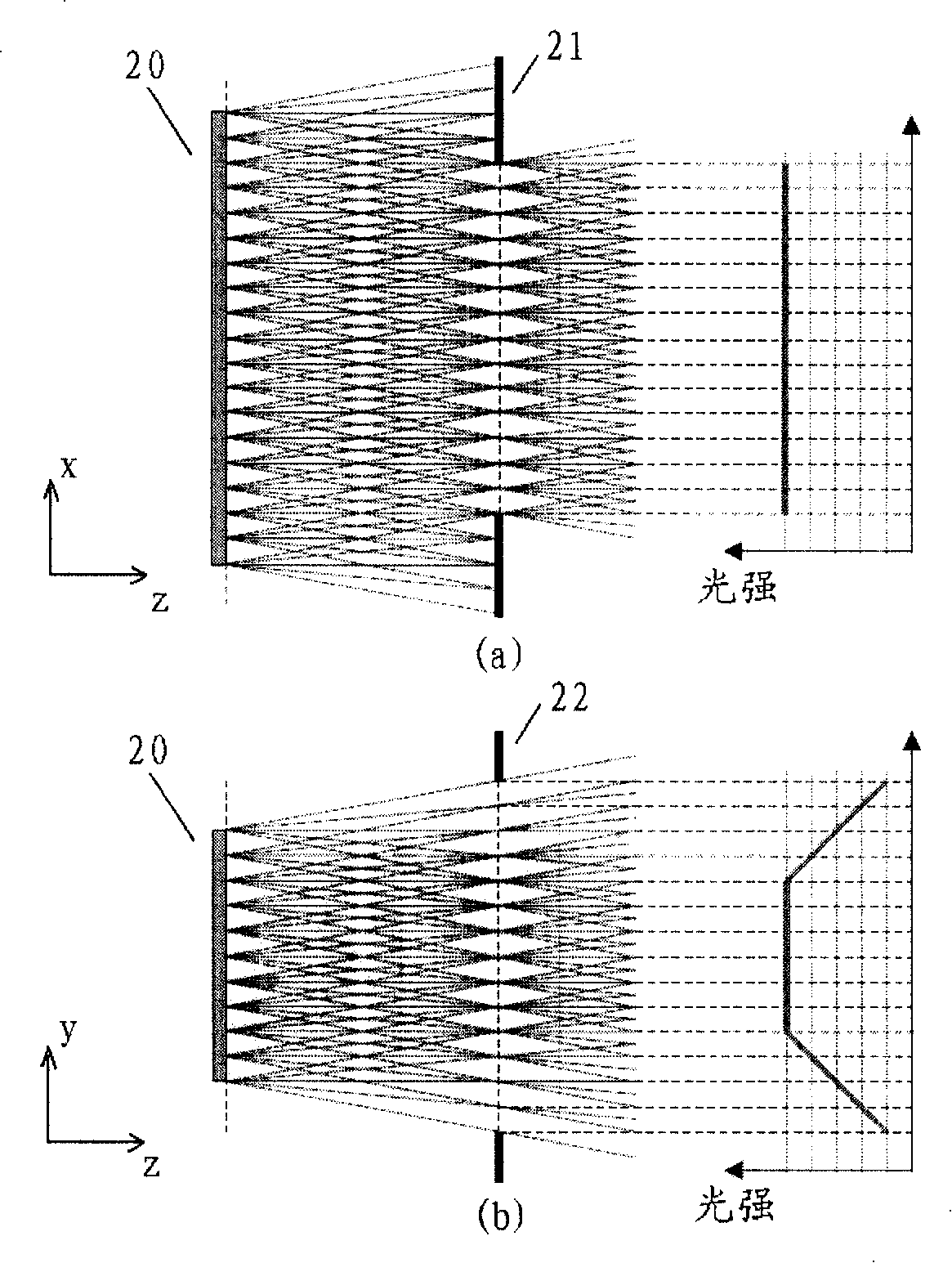
technical field [0001] The invention belongs to the field of microlithography, and relates to an illumination system for a semiconductor photolithography machine, in particular to a lithography illumination system containing an astigmatic microlens element. Background technique [0002] Photolithography (also known as microlithography) is used to fabricate semiconductor devices. Photolithography uses various wavelengths of light, such as ultraviolet (UV), deep UV, visible light, etc., to produce fine patterns in semiconductor device designs. Many kinds of semiconductor devices can be fabricated by photolithography, such as diodes, transistors and integrated circuits. [0003] In the manufacturing process of semiconductor devices, in order to meet the requirements of dose control of lithography machines, the illumination system of scanning lithography machines is usually required to form an illumination field with a one-dimensional trapezoidal light intensity distribution, a...

Claims


Application Information

Patent Timeline
IPC IPC(8): G03F7/20H01L21/027
CPCG03F7/7035
Inventor 李仲禹李铁军
Owner SHANGHAI MICRO ELECTRONICS EQUIP (GRP) CO LTD
Why Eureka
Try Eureka