
Eureka
For R&D, Eureka makes reading and utilizing patents & technical documents easy.
Eureka AIR
Designed for self-driven R&D workflows. Generate viable solutions, solve complex R&D challenges, empower your innovation with AI.

Eureka Materials
Designed for material experts only. Revolutionize your material R&D, from search, analyze, to developing new materials.

TechResearch
Generate reliable direction feasibility study reports for your R&D in just a few steps.

TechSeek
Discover and master advanced knowledge NOW. Basics, ideas, possibilities, all at once.

TechMind
As an expert in R&D Theories, TechMind can generates customized viable solutions instantly.

TechRisk
Analyze your overall solution with one click, know your potential R&D risks in advance.

TechMonitor
Get weekly tech updates, stay abreast of the latest tech innovations and key insights.
Method of fabricating a bipolar transistor
A technology for bipolar transistors, manufacturing processes, used in semiconductor/solid-state device manufacturing, semiconductor devices, electrical components, etc.
- Summary
- Abstract
- Description
- Claims
- Application Information
AI Technical Summary
Problems solved by technology
Method used
Image

Examples
Embodiment Construction
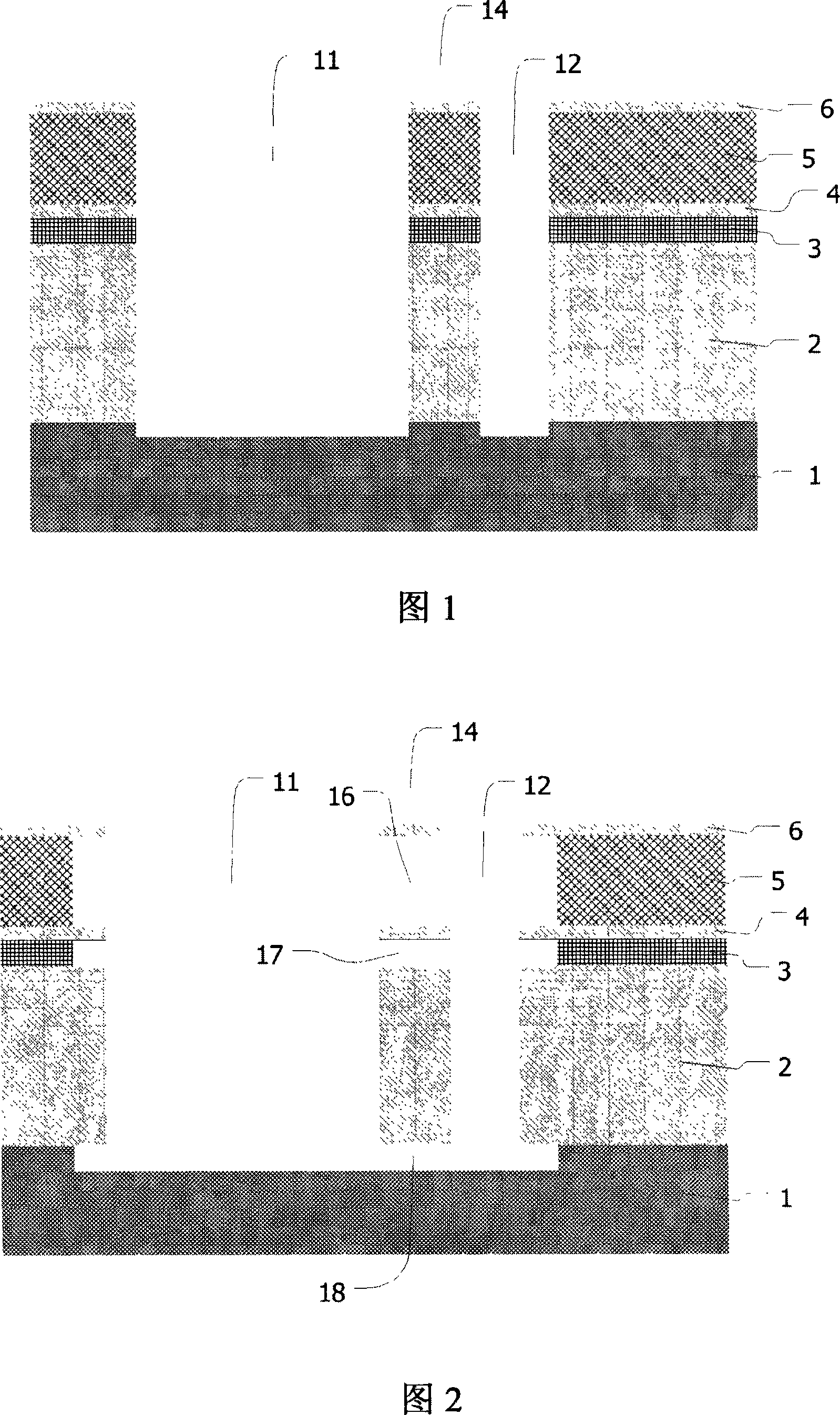
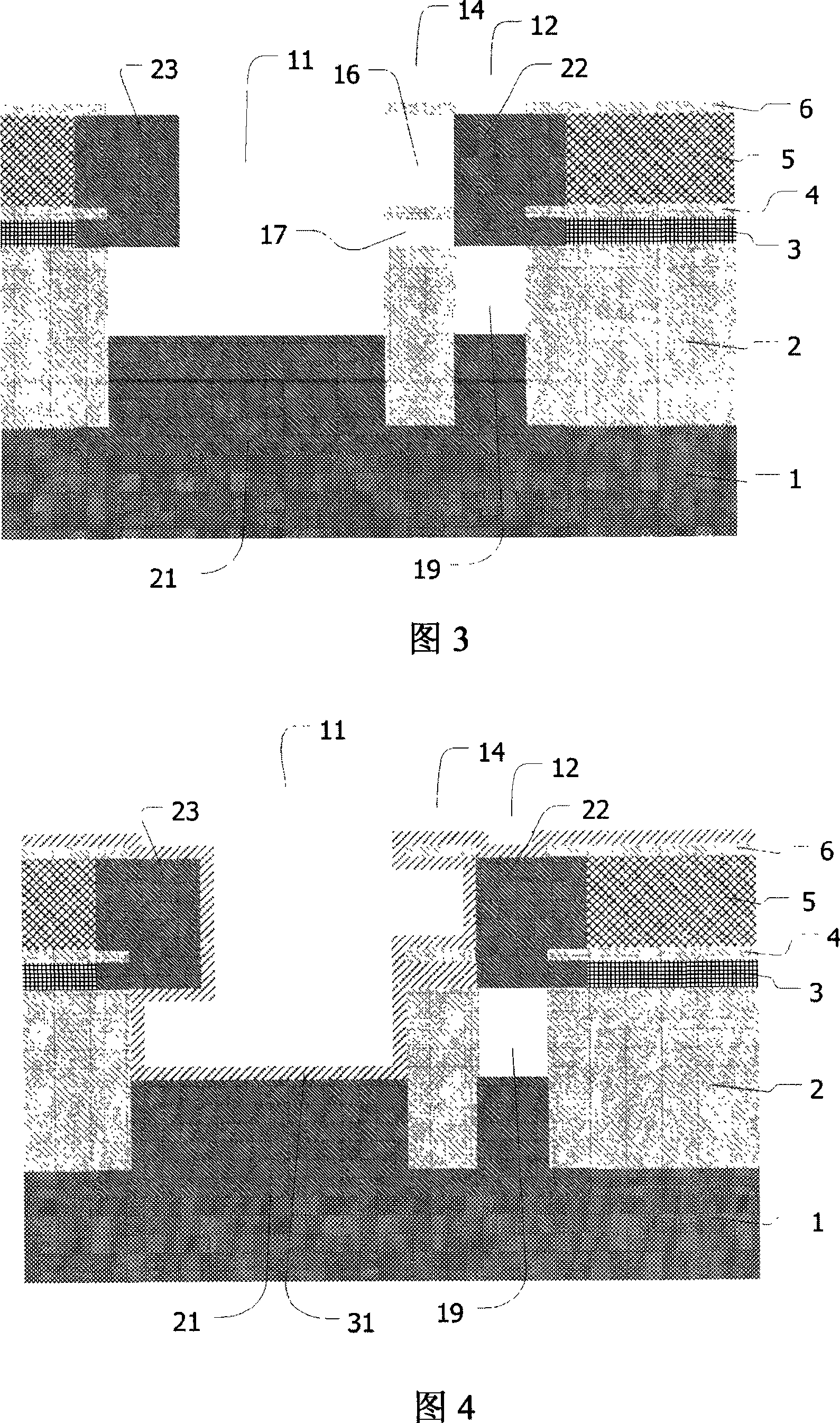
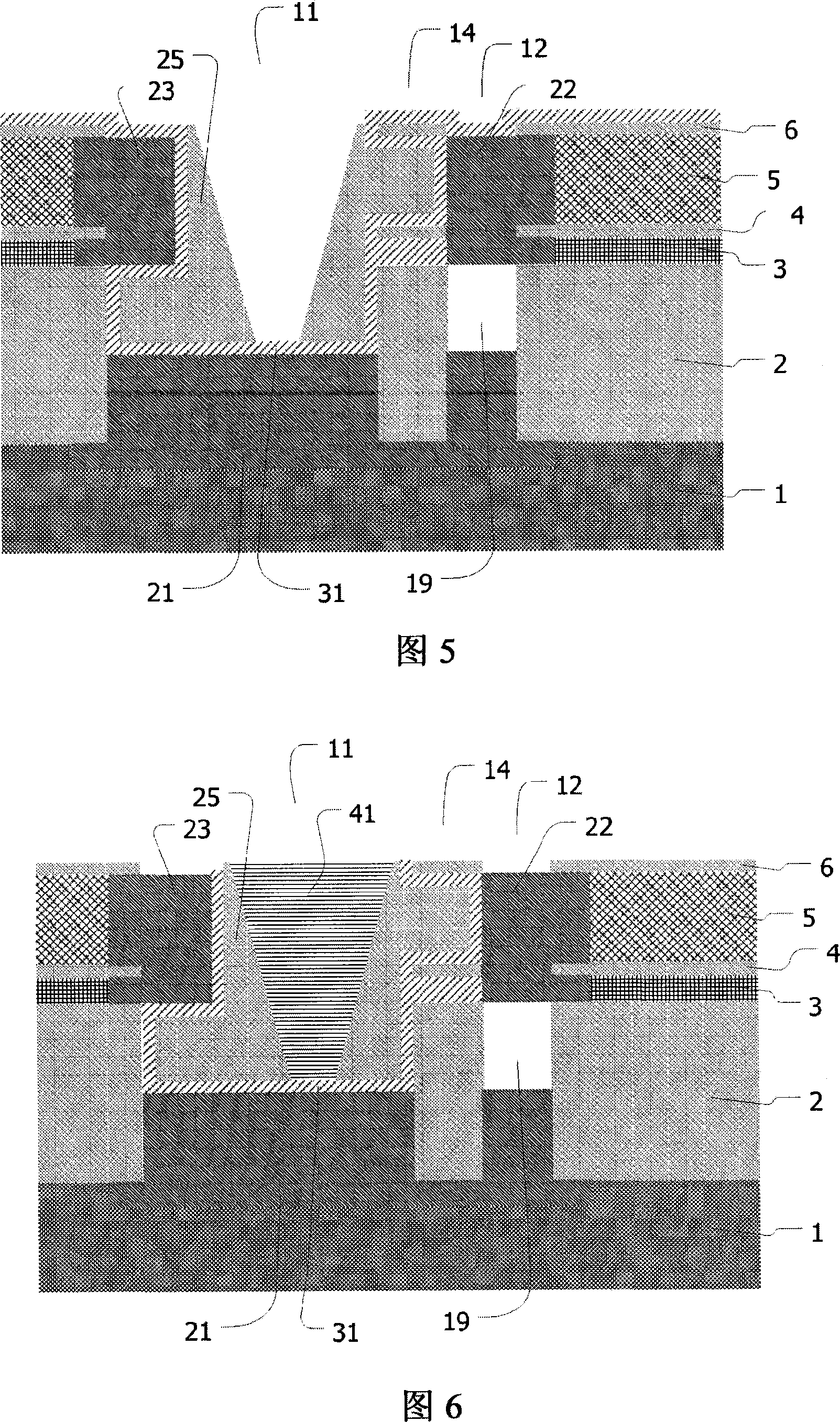
[0013] The starting point is a silicon-on-insulator (SOI) substrate comprising a silicon substrate region 1 on which a silicon dioxide region 2 and a silicon region 3 extend continuously. A silicon dioxide layer 4 is formed on the silicon region 3 using standard manufacturing techniques such as thermal oxidation processing. Polysilicon layer 5 is deposited on silicon dioxide layer 4 using standard manufacturing techniques. A hard mask layer 6 is then formed on the polysilicon layer 5, the hard mask layer 6 comprising eg silicon dioxide or another insulating material. The silicon dioxide layer 4 may include a gate oxide layer of a CMOS transistor, and the polysilicon layer 5 may include a gate electrode layer of a CMOS transistor. As shown in FIG. 1 , the first trench 11 and the second trench 12 are etched up to and including a part of the silicon substrate region 1 using standard photolithography and etching techniques. As a result, the first trench 11 and the second trench ...
PUM
 Abstract
Description
Claims
Application Information
 - R&D Engineer
- R&D Manager
- IP Professional
- Industry Leading Data Capabilities
- Powerful AI technology
- Patent DNA Extraction
Browse by: Latest US Patents, China's latest patents, Technical Efficacy Thesaurus, Application Domain, Technology Topic, Popular Technical Reports.
© 2024 PatSnap. All rights reserved.Legal|Privacy policy|Modern Slavery Act Transparency Statement|Sitemap|About US| Contact US: help@patsnap.com