Silicon based LCD unit and method for forming the same

A silicon-based liquid crystal and display technology, applied in the direction of instruments, electrical components, electric solid devices, etc., can solve problems such as leakage, affect the performance of switching circuits, reduce display refresh frequency, etc., and achieve the effect of reducing refresh frequency and increasing capacitance

Active Publication Date: 2008-06-11
SEMICON MFG INT (SHANGHAI) CORP +1
View PDF1 Cites 13 Cited by
  • Summary
  • Abstract
  • Description
  • Claims
  • Application Information

AI Technical Summary

Problems solved by technology

In order to reduce the refresh rate of the display, it is necessary to require the capacitance to be as large as possible. However, due to the limitation of the pixel area, if the proportion of the capacitance in the entire pixel is too high, it will inevitably affect the performance of the switching circuit. For example, because the design area of ​​the MOS transistor is reduced, the impact The insulation performance of MOS transistors is easy to cause leakage

Method used


Image

  • Silicon based LCD unit and method for forming the same
  • Silicon based LCD unit and method for forming the same
  • Silicon based LCD unit and method for forming the same

Examples


Embodiment Construction

[0026] Below by describing specific embodiment in detail according to accompanying drawing, above-mentioned object and advantage of the present invention will be clearer:

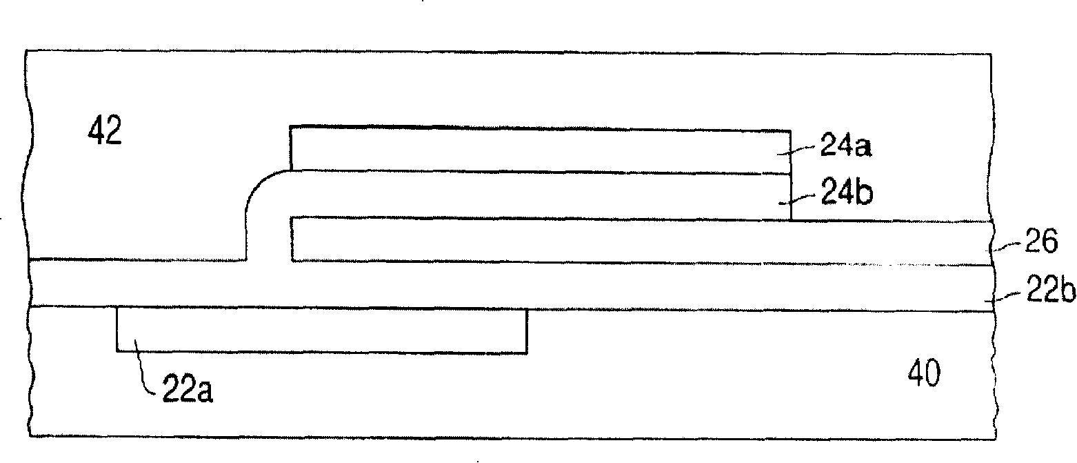
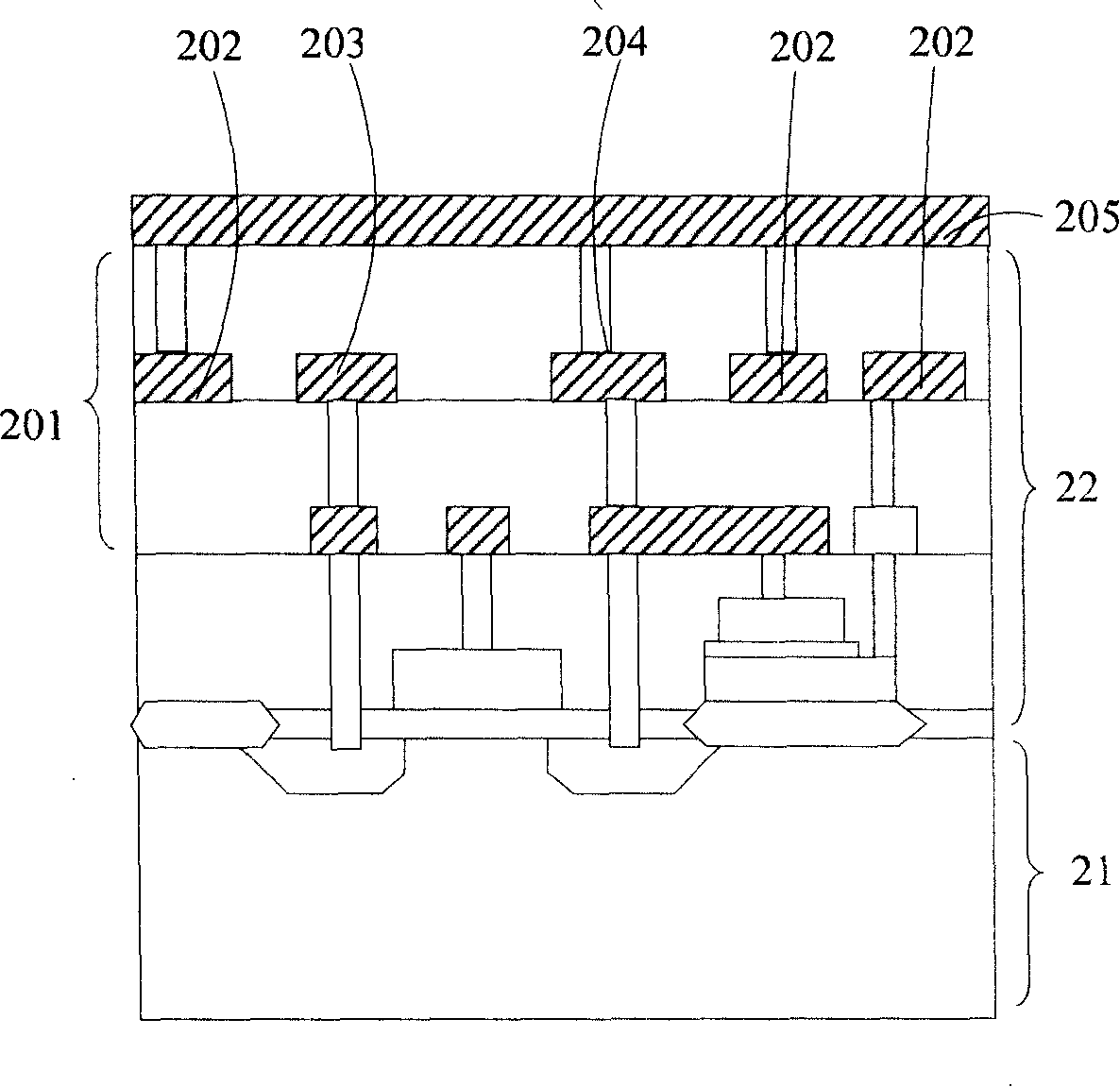
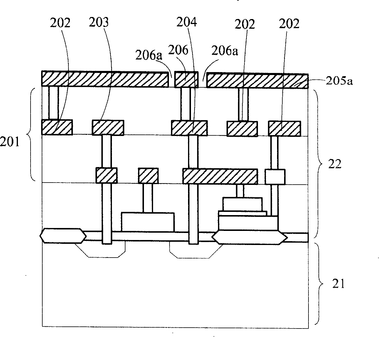
[0027] First, a method for forming a liquid crystal on silicon display unit is given, including forming a pixel switch circuit layer on a silicon substrate, the pixel switch circuit layer including a metal-oxide-semiconductor field effect transistor and a metal-oxide-semiconductor The source terminal of the field effect tube is connected in series with the first capacitor; a light shielding layer is formed on the pixel switch circuit layer; an insulating layer is formed on the light shielding layer; a micro-mirror layer is formed on the insulating layer, and the micro-mirror layer, the insulation The layer and the light-shielding layer form a capacitor, the micro-mirror layer is electrically connected to the source end of the metal-oxide-semiconductor field effect transistor, and the light-shielding layer is...


PUM

PropertyMeasurementUnit
thicknessaaaaaaaaaa

Abstract

A silicon-based liquid crystal display unit is provided, by grounding a light shielding layer located on a pixel switch circuit layer, a metal-insulating layer-metal (MIM) second capacitor composed by micro reflection micro reflecting mirror layer-insulating later-light shielding layer is formed, the second capacitance is connected with a first capacitance of the pixel switch circuit layer in parallel to be the capacitance of the pixel switch circuit layer together; the invention also provides a forming method of the silicon-based liquid crystal display unit. By fully utilizing the entire pixel area, the invention enlarges the capacitance, lowers the refresh rate of the silicon-based liquid crystal display unit. Simultaneously, the invention enlarges the design area of the switch circuit, designs high performance switch circuit according to different requirements and increases the design flexibility of the switch circuit. The invention also simplifies procedure of capacitance manufacture, so as to lower the total chip manufacture cost.

Description

technical field [0001] The invention relates to the field of semiconductors, in particular to a silicon-based liquid crystal display unit and a forming method thereof. Background technique [0002] In recent years, many new technologies have emerged in the liquid crystal (LCD) industry, among which the more popular technology is Liquid Crystal on Silicon (LCOS, Liquid Crystal on Silicon) technology. LCOS (LiquidCrystal on Silicon) is a new reflective micro LCD projection technology. Its structure is to grow a transistor on a silicon substrate, use a semiconductor process to make a drive panel (also known as CMOS-LCD), and then grind it on the transistor. The technology is ground and plated with aluminum as a micro-mirror to form a CMOS substrate, and then the CMOS substrate is bonded to the glass substrate containing the transparent electrode, and then the liquid crystal is pumped in for packaging and testing. [0003] Compared with traditional LCD and digital light process...

Claims


Application Information

Patent Timeline
Patent Type & Authority Applications(China)
IPC IPC(8): G02F1/1362H01L27/06H01L21/822H01L21/00
Inventor 黄河蒲贤勇毛剑宏陈轶群傅静洪中山向阳辉
Owner SEMICON MFG INT (SHANGHAI) CORP
Why Eureka
Try Eureka