Manufacture method of semiconductor device

A manufacturing method and semiconductor technology, applied in the fields of semiconductor/solid-state device manufacturing, electrical components, circuits, etc., can solve the problem of not being able to suppress the degradation of short-channel effect lifetime, increase process complexity and thermal budget cost, and improve device reliability. performance, reducing substrate leakage current and the effect of

Active Publication Date: 2008-06-25
SEMICON MFG INT (SHANGHAI) CORP +1
View PDF1 Cites 12 Cited by
  • Summary
  • Abstract
  • Description
  • Claims
  • Application Information

AI Technical Summary

Problems solved by technology

[0010] The problem solved by the present invention is that the manufacturing method of the semiconductor device in the prior art cannot suppress the short channel effect and the life of the input / output device is degraded, resulting in a defect in the reliability of the device. Improve the reliability of input / output devices while suppressing the substrate leakage current that may be caused by impact ionization

Method used


Image

  • Manufacture method of semiconductor device
  • Manufacture method of semiconductor device
  • Manufacture method of semiconductor device

Examples


Embodiment 1

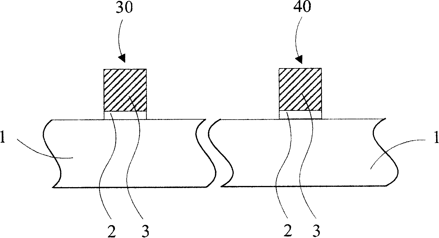
[0029] The present invention provides a method for manufacturing a semiconductor device, which includes the following steps: Picture 12 As shown, a semiconductor substrate is provided. The semiconductor substrate includes a core device area and an input / output device area. A gate dielectric layer and a gate dielectric layer are formed on the semiconductor substrate of the core device area and the input / output device area. The gate S200 on the layer; the gate is used as a mask, the first ion implantation S210 is performed in the semiconductor substrate in the core device area and the input / output device area; rapid thermal annealing is performed in the core device area and the input / output device area Low-doped source and drain regions S220 are formed in the semiconductor substrate on both sides of the gate dielectric layer; spacers S230 are formed in the gate dielectric layer of the core device region and the input / output device region and the sidewalls of the gate; The electrode...

Embodiment 2

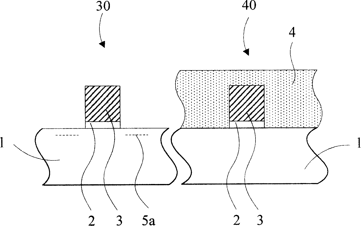
[0044] The present invention also provides a method for manufacturing a semiconductor device, which includes the following steps: Figure 13 As shown, a semiconductor substrate is provided. The semiconductor substrate includes a core device area and an input / output device area. A gate dielectric layer and a gate dielectric layer are formed on the semiconductor substrate of the core device area and the input / output device area. The gate S300 on the layer; using the gate as a mask, perform the first ion implantation S310 in the semiconductor substrate in the core device area and the input / output device area; using the gate as a mask, in the core device area and the input / output device Perform second ion implantation S320 into the semiconductor substrate in the region; perform rapid thermal annealing to form low-doped source and drain regions S330 in the semiconductor substrate on both sides of the gate dielectric layer in the core device region and the input / output device region; Th...

Embodiment 3

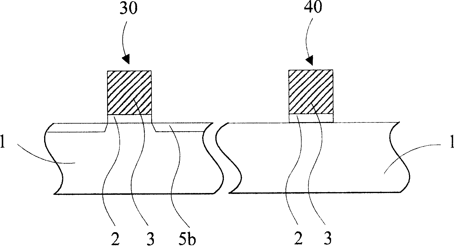
[0050] The present invention also provides a method for manufacturing a semiconductor device, which includes the following steps: Figure 14 As shown, a semiconductor substrate is provided. The semiconductor substrate includes a core device area and an input / output device area. A gate dielectric layer and a gate dielectric layer are formed on the semiconductor substrate of the core device area and the input / output device area. The gate S400 on the layer; using the gate as a mask, perform second ion implantation S410 in the semiconductor substrate in the core device area and the input / output device area; using the gate as a mask, in the core device area and the input / output device Perform first ion implantation S420 into the semiconductor substrate in the region; perform rapid thermal annealing to form low-doped source and drain regions S430 in the semiconductor substrate on both sides of the gate dielectric layer in the core device region and the input / output device region; The ga...


PUM


Abstract

The invention relates to a fabricating method of a semiconductor device. The method comprises the following steps: a semiconductor substrate comprising a core device region and input / output device region is provided, and gate dielectric layers and gatespositioned on the gate dielectric layers are formed on the semiconductor substrates of both the core device region and the input / output device region; the gates are taken as masks, and the first ion implantation is performed in the semiconductor substrates of both the core device region and the input / output device region; rapid thermal annealing is performed, low-doped source drain regions are formed in the semiconductor substrates at the both sides of the gate dielectric layers of both the core device region and the input / output device region; wall clearance are formed on both the gate dielectric layers of the core device region and the input / output device region and on the side walls of the gates; the gates and the spacers are taken as masks, and the third ion implantation is performed in the semiconductor substrates of the core device region and the input / output device region to form a heavily doped source drain region. The method can adjust the saturation current of the device, and improve the reliability of the input / output device.

Description

Technical field [0001] The present invention relates to the field of semiconductor technology, in particular to a manufacturing method of a semiconductor device. Background technique [0002] With the rapid development of semiconductor manufacturing technology, in order to achieve faster computing speed, greater data storage capacity and more functions, semiconductor chips are developing towards higher device density and high integration. Most of the peripheral circuits of semiconductor chips require high-voltage input / output devices, while core devices such as various memory devices need to operate at low voltages. In order to maximize the performance of the devices, the channel length of the core devices is shortened, resulting in short Channel region and short channel effect. In order to avoid the short channel effect, a lightly doped source / drain (LDD) structure is usually adopted. [0003] As the channel length of the core device shrinks, in order to obtain the required driv...

Claims


Application Information

Patent Timeline
Patent Type & Authority Applications(China)
IPC IPC(8): H01L21/8234
CPCH01L21/823418H01L21/82345H01L29/6659
Inventor 王津洲赵猛
Owner SEMICON MFG INT (SHANGHAI) CORP
Why Eureka
Try Eureka