Method for evaluating development capability

A capability and developing machine technology, applied in electrical components, semiconductor/solid-state device manufacturing, circuits, etc., can solve problems such as cost increase, photoresist residue, affecting the quality of semiconductor devices, etc., to achieve the effect of cost reduction and yield improvement

Inactive Publication Date: 2008-07-02
SEMICON MFG INT (SHANGHAI) CORP
View PDF1 Cites 5 Cited by
  • Summary
  • Abstract
  • Description
  • Claims
  • Application Information

AI Technical Summary

Problems solved by technology

[0007] In the existing photolithography process, photoresist residues are usually caused by insufficient development, which affects the quality of subsequent semiconductor devices; in order to evaluate the developing ability of the developing machine—the effect of develo

Method used


Image

  • Method for evaluating development capability
  • Method for evaluating development capability
  • Method for evaluating development capability

Examples


Embodiment Construction

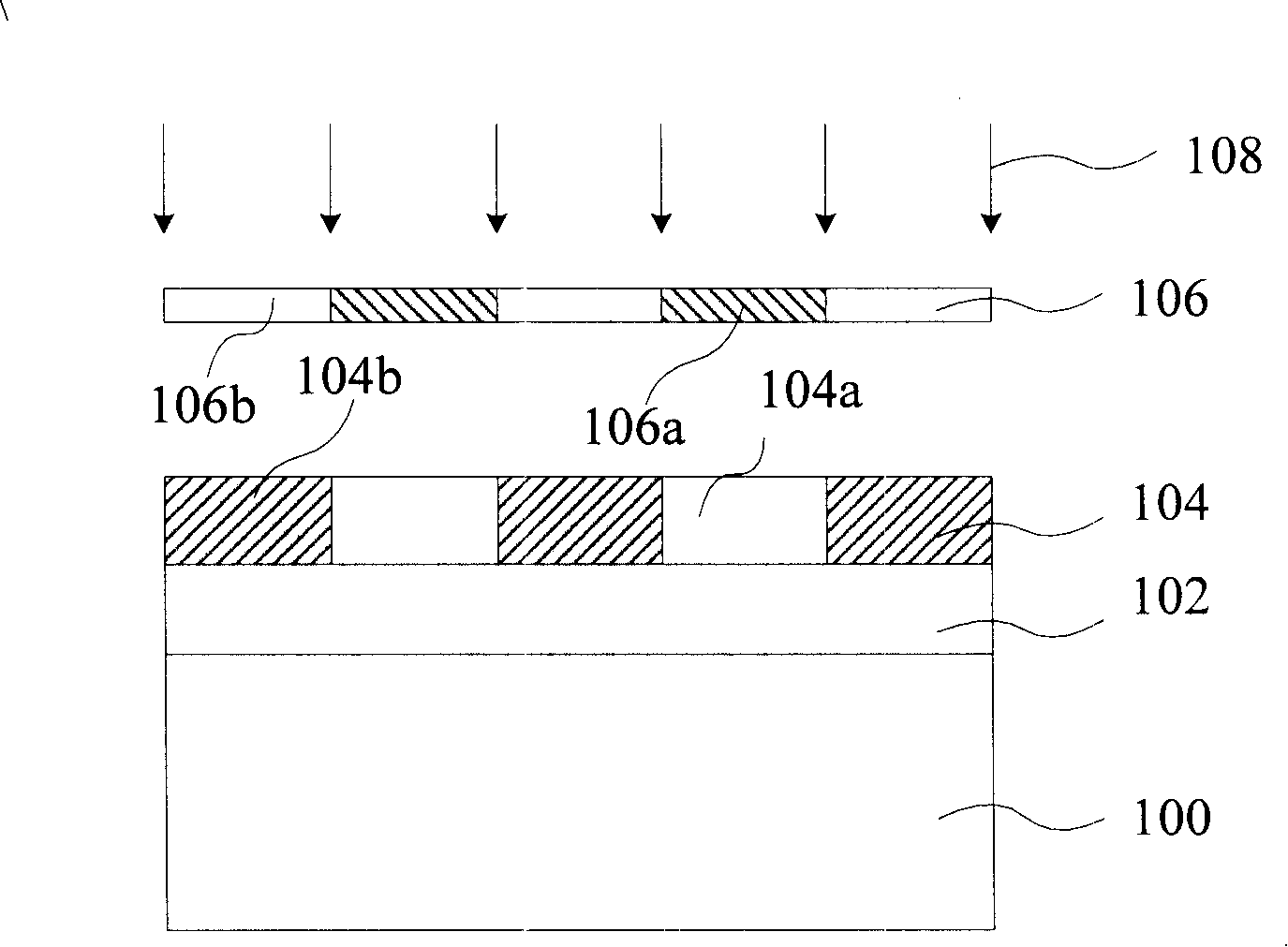
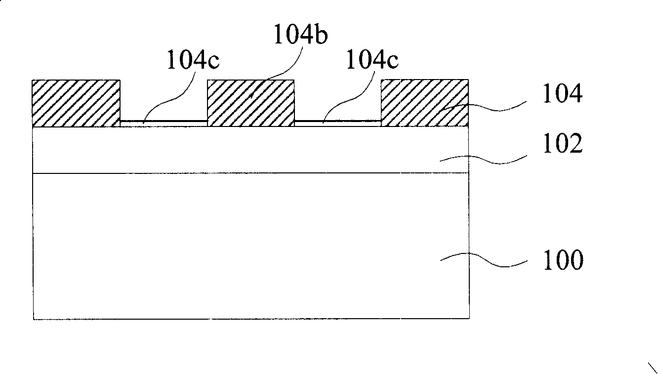
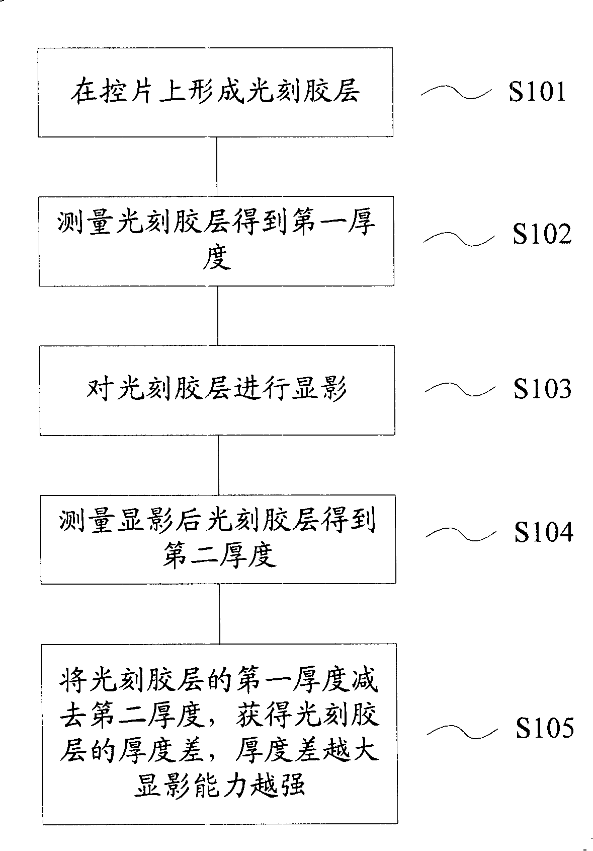
[0020] In the existing photolithography process, photoresist residues are usually caused by insufficient development, which in turn affects the quality of subsequent semiconductor devices; usually photoresist residues are caused by insufficient development, which in turn affects the quality of subsequent semiconductor devices; Evaluate the developing ability of the developing machine—the effect of developing photoresist. Generally, after the formed semiconductor device is sliced, it is made into a scanning electron microscope sample to observe whether the photoresist remains, which will increase the cost and affect the quality of the semiconductor device. Yield. The present invention forms a photoresist layer on the control sheet, measures the first thickness of the photoresist layer before development, measures the second thickness of the photoresist layer after development, and subtracts the second thickness from the first thickness to obtain Find the developing ability of t...


PUM


Abstract

A method of assessing developing capacity comprises the following steps: a photoresist layer is formed on a control wafer; a first thickness is obtained by measuring the photoresist layer; the photoresist layer is developed; a second thickness is obtained by measuring the developed photoresist layer; the thickness difference of the photoresist layer is obtained by subtracting the second thickness from the first thickness of the photoresist layer; the greater the thickness difference is, the stronger the developing capacity is. With the steps, the cost of assessing the developing capacity of a developer is reduced; at the same time, the quality of the semiconductor devices of the actual process is not affected, and the yield is increased.

Description

technical field [0001] The invention relates to the manufacture of semiconductor devices, in particular to a method for evaluating developing ability in the photolithography process of semiconductor devices. Background technique [0002] As the integration level of semiconductor devices is getting higher and higher, the line width of semiconductor devices is getting thinner and thinner, and the requirements for photolithography are also higher. [0003] For the method of forming a photoresist pattern in the existing photolithography process, please refer to the technical solution disclosed in the Chinese Patent No. 01140031. Such as Figure 1A As shown, first a wafer 100 is provided, on which a semiconductor device structure (not shown) is formed; on the wafer 100 with the semiconductor device structure, a layer 102 to be etched is formed, and the layer 102 to be etched is such as a metal layer , a polysilicon layer, a silicon nitride layer or a silicon oxide layer; a photo...

Claims


Application Information

Patent Timeline
IPC IPC(8): G03F7/16G03F7/20G03F7/26H01L21/027
Inventor 郁志芳章磊余云初王跃刚
Owner SEMICON MFG INT (SHANGHAI) CORP
Why Eureka
Try Eureka