Detection system and method

A detection method and detection system technology, applied in semiconductor/solid-state device testing/measurement, optics, instruments, etc., can solve problems such as unfavorable production efficiency and time-consuming 1 hour, and achieve the effect of improving efficiency and avoiding pauses

Inactive Publication Date: 2008-07-02
SEMICON MFG INT (SHANGHAI) CORP
View PDF1 Cites 5 Cited by
  • Summary
  • Abstract
  • Description
  • Claims
  • Application Information

AI Technical Summary

Problems solved by technology

The setting of each detection process takes about 1 hour, and the lithography steps of a new product are at least 20 steps, and every time the detection process is set, the entire production process is in a stopped state, which means However, just because of the setup steps of the overlay inspection process, the completion of each new product will be delayed by a day or so, which is not good for the improvement of production efficiency.

Method used


Image

  • Detection system and method
  • Detection system and method
  • Detection system and method

Examples


Embodiment Construction

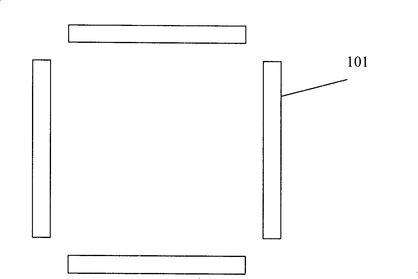
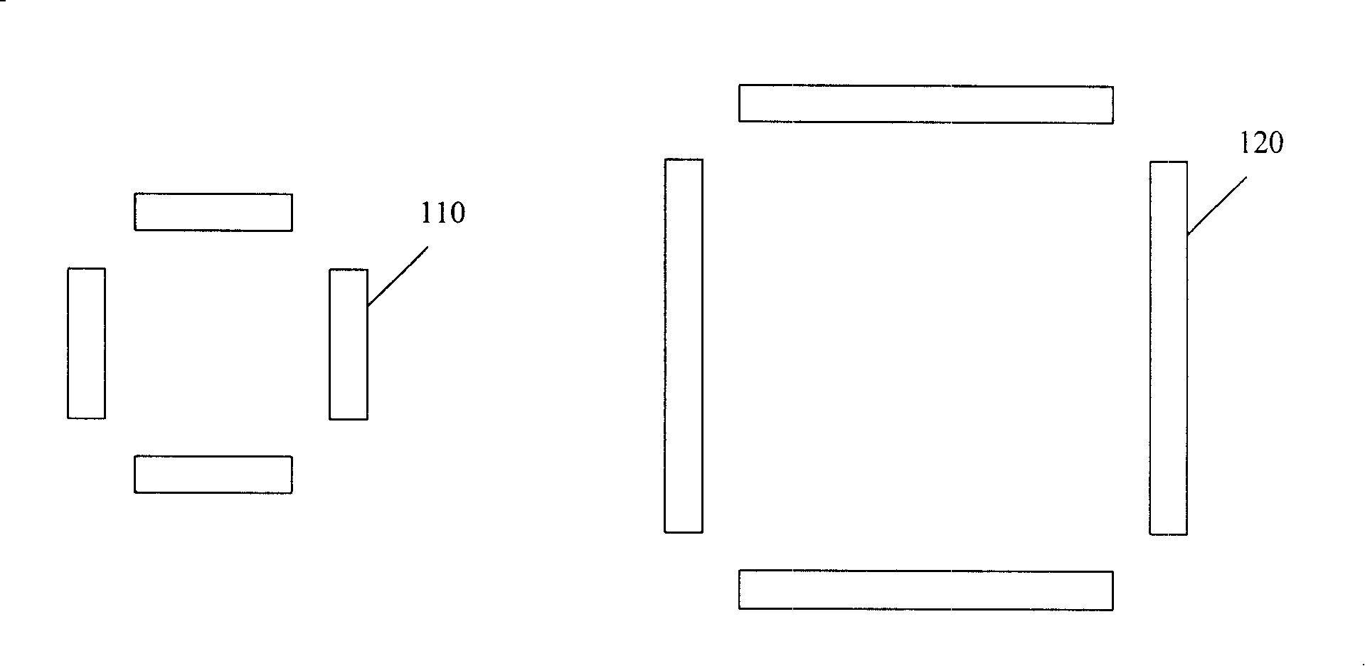
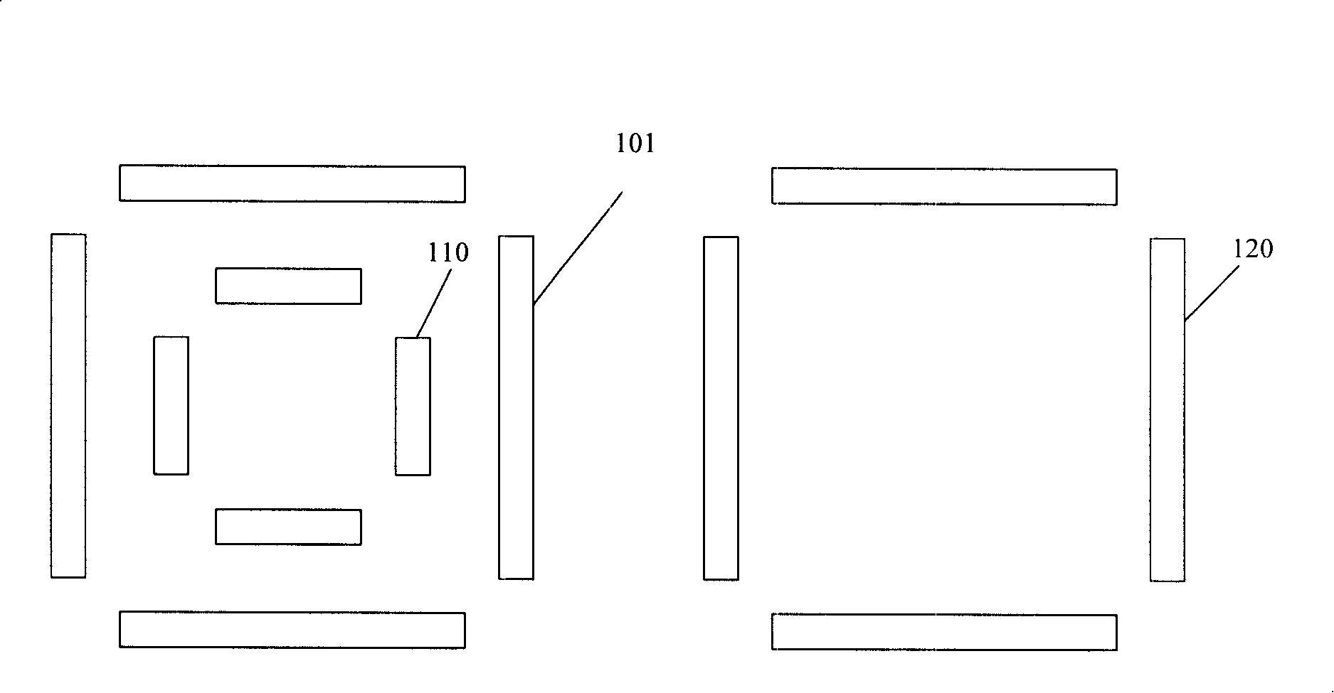
[0038] In order to make the above objects, features and advantages of the present invention more comprehensible, specific implementations of the present invention will be described in detail below in conjunction with the accompanying drawings.

[0039] Note that processing method of the present invention can be widely applied in many applications, below is only described by preferred embodiment, certainly the present invention is not limited to this specific embodiment, those of ordinary skill in the art can understand Known general substitutions are undoubtedly covered by the protection scope of the present invention.

[0040] In addition, the present invention has been described in detail using schematic diagrams. When describing the embodiments of the present invention in detail, for the convenience of illustration, the schematic diagrams will not be partially enlarged according to the general scale, which should not be used as a limitation of the present invention. In addit...


PUM


Abstract

The invention discloses a detection method and a detection system. The detection method comprises the steps that: a process group at least containing one detection process is established and the data of the wafer to be measured is acquired; the detection process, the detection object of which is the same as that of the wafer to be measured, is selected as a first detection process and the first detection process is adjusted utilizing the data of the wafer to be measured so as to generate a second detection process; the second detection process is executed to accomplish the detection of the wafer to be measured. The adoption of the detection system of the detection method of the invention can set the steps and conditions for detection under the circumstance that the wafer is not provided, thereby avoiding the process flow from being stopped due to the setting of the detection process and enhancing the production efficiency.

Description

technical field [0001] The invention relates to the technical field of semiconductor device manufacturing, in particular to a detection method and a detection system. Background technique [0002] The integrated circuit manufacturing process is a planar manufacturing process, which combines photolithography, etching, deposition, ion implantation and other processes to form a large number of various types of complex devices on the same substrate and connect them to each other to have a complete electronic functions. Among them, problems in any step of the process may lead to the failure of the production of the circuit. Therefore, it is often necessary to detect the production results of each step of the process in the process, especially for the photolithography process, because it can be reworked and repaired. The problem that arises, this detection process is more critical. [0003] With the rapid development of the semiconductor manufacturing process, the inspection pro...

Claims


Application Information

Patent Timeline
IPC IPC(8): H01L21/66H01L21/027G03F7/20G03F9/00
Inventor 张轲
Owner SEMICON MFG INT (SHANGHAI) CORP
Why Eureka
Try Eureka