A maintenance method of plasma etching device

A kind of etching equipment and plasma technology, applied in the direction of electrical components, semiconductor/solid-state device manufacturing, circuits, etc., can solve the problems of lower yield, lower efficiency, and affect the silicon wafer processing process, so as to save time, improve efficiency, The effect of ensuring the quality of silicon wafer processing

Active Publication Date: 2010-09-01
BEIJING NAURA MICROELECTRONICS EQUIP CO LTD
View PDF3 Cites 0 Cited by
  • Summary
  • Abstract
  • Description
  • Claims
  • Application Information

AI Technical Summary

Problems solved by technology

Excessively large maintenance intervals lead to changes in process results due to changes in process status, resulting in poor wafer processing quality and low yield; excessively small maintenance intervals make equipment maintenance too frequent, affecting the normal wafer processing process and wasting time ,Reduce efficiency

Method used


Image

  • A maintenance method of plasma etching device
  • A maintenance method of plasma etching device
  • A maintenance method of plasma etching device

Examples


specific Embodiment approach

[0053] Its specific implementation method comprises the following steps:

[0054] In the first step, the corresponding relationship between the performance parameters of the products in the plasma etching equipment and the surface roughness inside the reaction chamber of the plasma etching equipment is established.

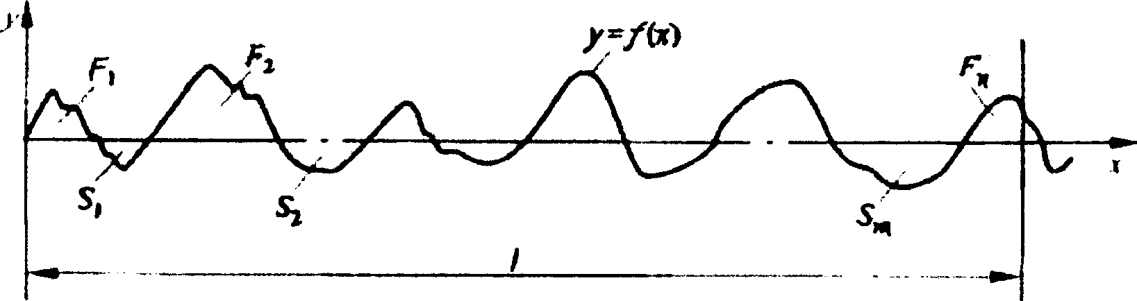
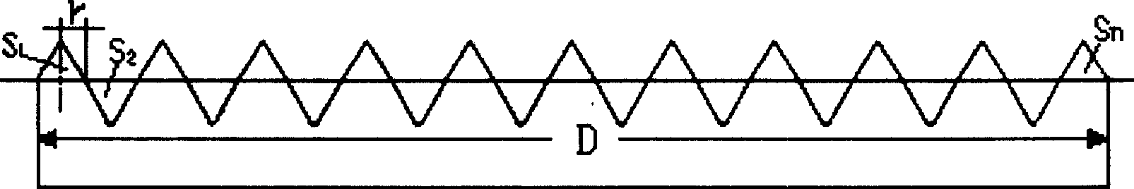
[0055] In this process, the corresponding relationship between the inner surface area S of the reaction chamber and the roughness value Ra of the inner surface of the reaction chamber can be established first, including:

[0056] (1) Establishing a mathematical model of the surface area Sn of the microscopic particles on the inner surface of the reaction chamber and its surface roughness value Ra, Sn=fn(Ra).

[0057] Firstly, the model of the surface particles of the quartz component is established, and the particle radius r under different roughness is calculated according to the definition of roughness. The quartz components in the etching machine mainly refer ...


PUM

PropertyMeasurementUnit
surface roughnessaaaaaaaaaa

Abstract

The invention relates to a maintenance method of plasma etching equipment, the corresponding relationship of the performance parameters of the products of the plasma etching equipment and the roughness of the inner surface of a reaction cavity body of the plasma etching equipment is firstly established; the performance parameters of the products of the plasma etching equipment are detected, the roughness of the inner surface of the reaction cavity body is judged whether to meet the process requirements according to the corresponding relationship, the reaction cavity body is replaced when the roughness does not meet the requirements. The replacement time of a vulnerable part of the plasma etching equipment can be predicted accurately relatively by the method, so as to replace the vulnerable part of the plasma etching equipment in time, ensure the processing quality of a silicon wafer, maintain the normal process of the silicon wafer, save the time and improve the efficiency.

Description

technical field [0001] The invention relates to the technical field of microelectronic etching, in particular to a method for maintaining plasma etching equipment. Background technique [0002] With the development of microelectronics technology, semiconductor chip processing technology is becoming more and more stringent, the technology node has been from 180nm to 65nm, even below 45nm, and the size of silicon wafers has also increased from 200mm to 300mm. Therefore, the process requirements for silicon wafers are becoming more and more stringent. . The etching process is one of the most complex processes in semiconductor processing. The state of the plasma and various process parameters during the etching process are directly related to the etching result. [0003] In the structure of the plasma etching machine, the quartz parts directly contact the plasma, which is closely related to the state of the reaction chamber. The roughness of the surface will increase with the i...

Claims


Application Information

Patent Timeline
Patent Type & Authority Patents(China)
IPC IPC(8): H01L21/00H01L21/3065C23F4/00
Inventor 杨峰
Owner BEIJING NAURA MICROELECTRONICS EQUIP CO LTD
Why Eureka
Try Eureka