Laser annealing technique on the wafer back of IGBT high voltage power device

A high-voltage power device and laser annealing technology, which is applied in the manufacture of semiconductor/solid-state devices, electrical components, circuits, etc., can solve the problems of suboptimal device characteristics, no better process plan, and large conduction series resistance, etc., to overcome The effect of bad influence

Active Publication Date: 2008-07-09
TSINGHUA UNIV
View PDF0 Cites 13 Cited by
  • Summary
  • Abstract
  • Description
  • Claims
  • Application Information

AI Technical Summary

Problems solved by technology

However, after ion implantation, the implanted impurities need to be activated by annealing. In terms of annealing process, there is no better process plan, so the on-series resistance of high-voltage IGBT devices is still relatively large, and the device characteristics are not ideal.

Method used


Image

  • Laser annealing technique on the wafer back of IGBT high voltage power device

Examples


Embodiment Construction

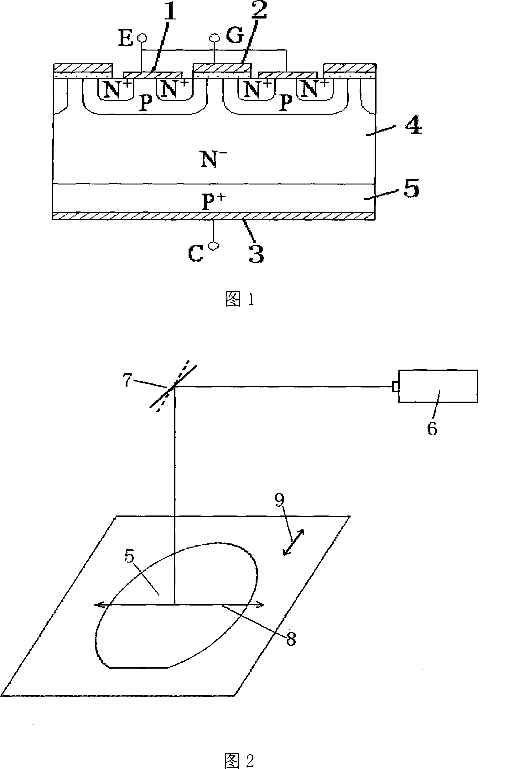
[0016] The invention provides a laser annealing process on the back side of an IGBT high-voltage power device wafer by adopting a laser scanning method. The present invention will be described below in conjunction with the accompanying drawings.

[0017] Figure 1 is a schematic diagram of the structure of an IGBT high voltage device. Among them, one side of the emitter 1 of the IGBT high-voltage power device is the control gate 2, and the bottom of the control gate 2 is the channel region, N - The drift region 4 of the type is located below the above device structure, and the P-type implanted doped layer on the back side of the silicon wafer 5 is used as the collection area 3 of the IGBT high-voltage power device. A good ohmic contact is formed between the P-type implanted doped layers.

[0018] Fig. 2 is a schematic diagram of a device for realizing laser scanning annealing. The specific process is illustrated as follows:

[0019] 1. Use a continuous laser with a waveleng...


PUM


Abstract

The invention discloses a wafer back surface laser annealing process of an IGBT high-voltage power device, which pertains to the semiconductor manufacturing technical scope. The invention adopts a scanning mode to carry out the laser annealing, a silicon wafer back surface is controlled to do the reciprocating uniform linear motion along the vertical direction of a long strip-shaped laser spot, so as to form the laser spot to carry out the scanning of the entire area of the silicon wafer back surface, increase the temperature of a surface layer of the silicon wafer back surface and generate the uniform annealing effect. The usage of the proposal of the invention can solve the problem that a P-shaped doping layer can not carry out good annealing processing after the ion injection, so a good ohmic contact is formed between a collector metal layer and the P-shaped doping layer which is close to the silicon wafer. The invention uses a laser with the shorter wavelength, the penetration depth of the laser on the silicon wafer back surface is limited, the invention can not only faster realize the activation of impurities, but also generate the adverse effects on other structural parts of the IGBT high-voltage power device; the usage of the technology can obtain the IGBT high-voltage power device with the smaller on-state resistance.

Description

technical field [0001] The invention belongs to the technical scope of semiconductor manufacturing, and in particular relates to a laser annealing process on the back of an IGBT high-voltage power device wafer, which uses a laser annealing method to implement ion implantation doping annealing process technology. Background technique [0002] IGBT is an insulated gate bipolar transistor. This type of device has good switching characteristics due to the combination of the advantages of field effect transistors and bipolar transistors. IGBT high-voltage power devices are currently mainly used in high-voltage, high-current and other power applications. [0003] The structure of an IGBT high-voltage power device is shown in Figure 1. Among them, the device can withstand high voltage because of the thicker N - layer 4 sake, this N - The thicker the layer, the higher the withstand voltage of the device. Usually, when N - When the layer is not too thick, it can be made by epita...

Claims


Application Information

Patent Timeline
Patent Type & Authority Applications(China)
IPC IPC(8): H01L21/331H01L21/268
Inventor 刘志弘严利人周卫刘朋
Owner TSINGHUA UNIV
Why Eureka
Try Eureka