

High energy beam polysilicon purifying device
A technology of polysilicon and high-energy beams, which is applied in the direction of silicon compounds, inorganic chemistry, non-metallic elements, etc., can solve problems such as environmental pollution, high cost, and large energy consumption
- Summary
- Abstract
- Description
- Claims
- Application Information
AI Technical Summary
Problems solved by technology
Method used
Image

Examples
Embodiment Construction
[0020] The present invention will be further described in detail below in conjunction with the accompanying drawings.
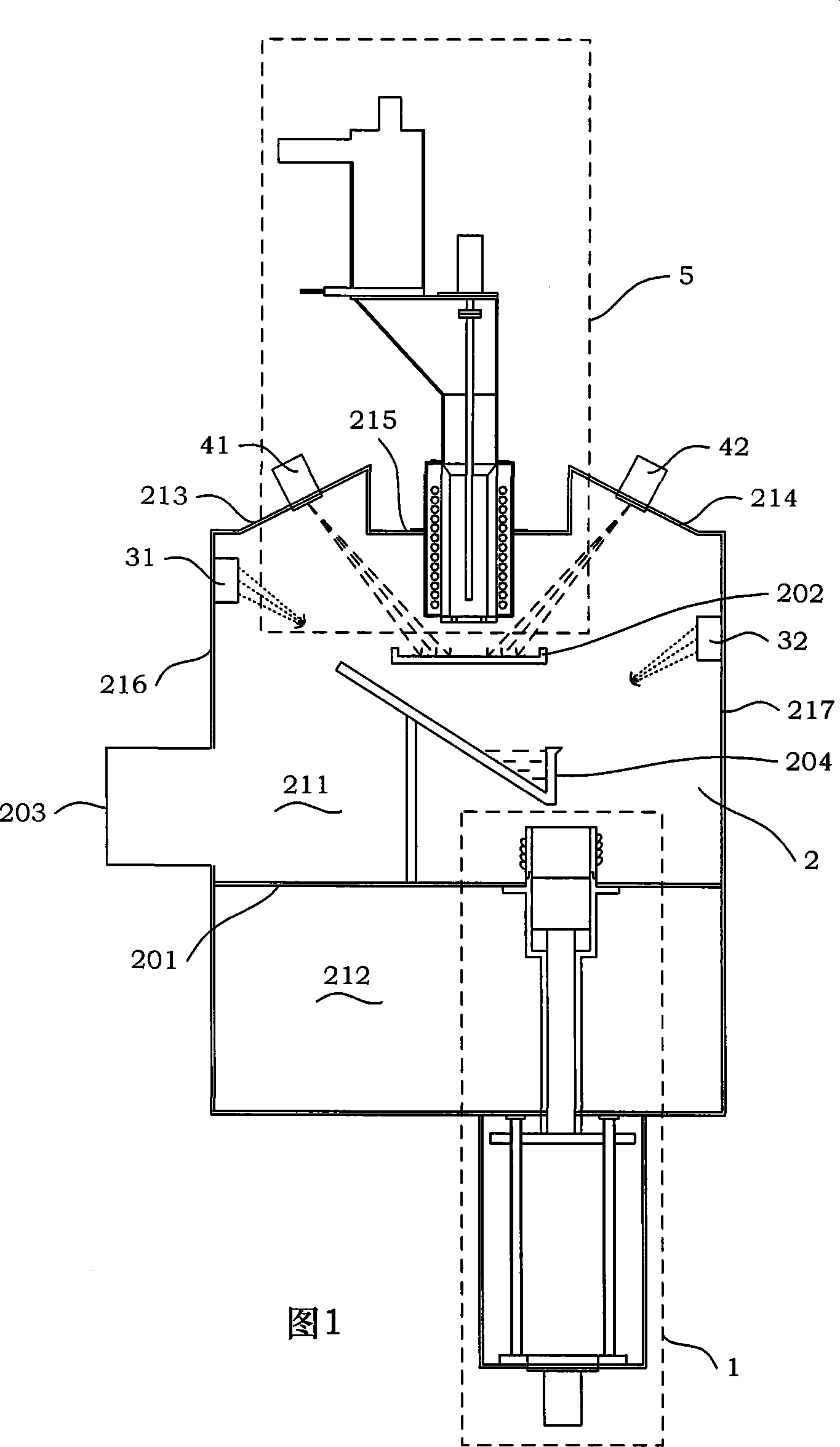
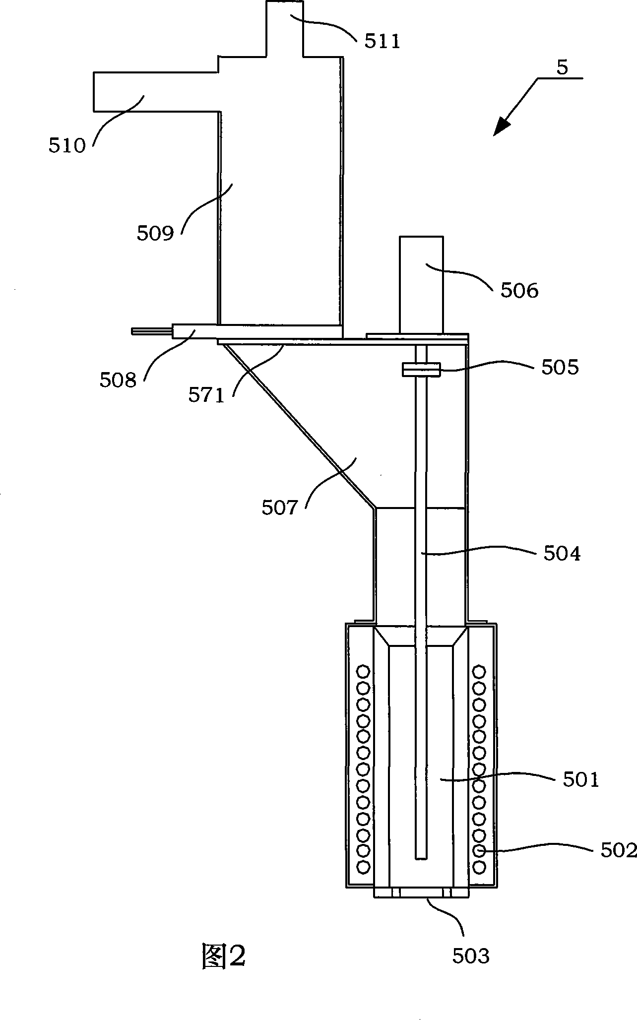
[0021] Referring to Fig. 1, the present invention is a four-in-one high-energy beam polysilicon purification device integrating isovacuum electromagnetic induction smelting, electron beam smelting, ion smelting, and directional solidification. The purification device includes a directional solidification unit 1, a vacuum Chamber 2, plasma smelting unit, electron beam smelting unit, vacuum electromagnetic induction smelting unit 5; vacuum electromagnetic induction smelting unit 5 is installed on the concave surface 215 of vacuum chamber 2; A electron gun 41 of electron beam smelting unit is installed in vacuum chamber 2 On the left inclined plane 213 of the vacuum chamber 2, the B electron gun 42 is installed on the right inclined plane 214 of the vacuum chamber 2; On the right housing 217 ; the connection seat 182 of the directional solidification unit 1 is i...
PUM
 Abstract
Description
Claims
Application Information